光技術情報誌「ライトエッジ」No.21(2001年4月発行)
TPCAショー2000セミナー
(2000年11月)
Most Advanced Technology Trend
in
Step-&-Repeat Projection Exposure System
for Printed-Circuit Boards
Yoneta Tanaka , Toshiyuki Mastuki , Jun Homma
Project Promotion Division Systems Division USHIO INC.
6409 Motoisikawa-cho Aoba-ku Yokohama JAPAN
E-mail: TANAKAYN@mail.ushio.co.jp
General:
There are three typical challenges in manufacturing printed-circuit boards: enhancement of the overlay accuracy of the exposure pattern, decrease in the fine pattern size, and enhancement of the product yield. To meet these challenges, the step-and-repeat projection exposure method using a projection lens is effective. As its most prominent feature, the step-and-repeat projection exposure method allows non-contact patterning. It also can measure the expansion/contraction ratio of the actual pattern at each shot so as to allow projection of the mask at the corresponding expansion/contraction ratio.
It can be considered as essential in the future to introduce the step-and-repeat projection exposure system into production of the interposer boards for BGAs/CSPs, which are expected to increase in its production volume, and the printed-circuit boards for digital equipment.
This paper presents basic studies of Step -&-Repeat Projection Exposure System and machine performance due to actual PWB panel behavior . Furthermore the road map for ushio development of the exposure machine is also described.
Introduction:
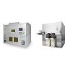
In recent years, high resolution and high overlay accuracy have been required for printed-circuit boards such as MPU packages. We at USHIO developed a step-and-repeat projection exposure system for printed-circuit boards aiming at the achievement of high resolution, high overlay accuracy, and enhancement of the product yield.
The standard at which the step-and-repeat projection exposure method becomes effective is for products that require an overlay accuracy of within ±30 µm and a minimum line width of within 50 µm. In addition, this method is effective for cases in which a mask defect has caused a series of workpiece defects.
A printed-circuit board expands or contracts asymmetrically during production. The conventional system has reduced deterioration in the overlay accuracy by correcting the mask. However, because the expansion/contraction amount varies in different areas within the same board, the conventional system has a limit in enhancement of the overlay accuracy and yield. It therefore can be considered that use of the step-andrepeat projection exposure method and the auto scale function is essential for exposure of printed-circuit boards at high accuracy.
In addition, the projection exposure system generally uses an off-axis alignment method, which has difficulty in implementing closed-loop alignment. We have solved this problem by utilizing on-axis TTL alignment using a non-exposure wavelength.
We consider that application of the step-and-repeat projection exposure system to future manufacturing of printed-circuit boards is the most important challenge.
1. BASIC SYSTEM PERFORMANCE
1-1. Projection Lens and Resolution
The projection lens used for USHIO's exposure systems has an effective diameter of Φ200 mm. A projection lens with the effective diameter of Φ150 mm is also manufactured for high-resolution systems. In addition, a large-area exposure system using the projection lens with the effective diameter of Φ250 mm is scheduled to be released in 2001. The resolution and main wavelengths of these systems range from 5 µmL/S at 365 nm to 12 µm at 365 nm, 405 nm, and 436 nm.
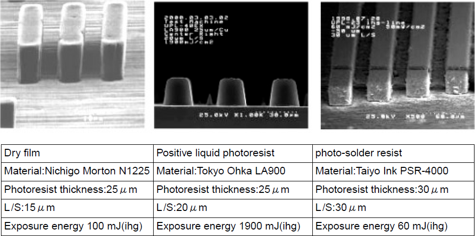
Resolution is mostly specified as t he minimum line width to be resolved of a dry film photoresist. However, for the actual process, a photosolder photoresist or photosensitive insulator is mostly used.
As resolution samples of the process performed by USHIO's exposure system, the following shows SEM photographs of three photoresist types processed by the projection exposure method.
The diameter of the lens can be easily increased by using a non-telecentric lens. However, though a nontelecentric lens can obtain a satisfactory depth of focus, it causes distortion of the exposure pattern on a concave-convex workpiece. Therefore, the projection lens mounted on USHIOユs exposure system is of telecentric type.
1-2. Alignment Method and Accuracy
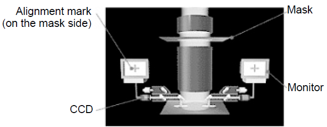
As the alignment method, USHIO's exposure system utilizes on-axis TTL alignment using a non-exposure wavelength. The projection lens is usually designed to obtain the required resolution with the exposure light (to correct the aberration). For this reason, off-axis alignment is generally used to partially radiate the exposure wavelength as an alignment light. Use of the exposure wavelength for alignment causes the area surrounding the alignment mark to be exposed during alignment. If the required resolution is low, it can be considered to use the projection lens that corrects the aberration with two lines: the exposure wavelength and the non-exposure wavelength (generally 546 nm). However, as the required resolution becomes higher and the exposure area becomes larger, this method may not be used.
On-axis TTL alignment using a non-exposure wavelength is effective to solve this problem. USHIO's method works as follows:
Procedure 1: Calibration of th e Mask
Procedure 1 is the method for calibrating the relative positions of the mask and the vision of the alignment microscope. The mask image can be directly observed by the exposure wavelength. Under this condition, there is only the mask alignment ma rk in the vision of the detection system. Therefore, is not necessary to consider interference with the workpiece alignment mark.
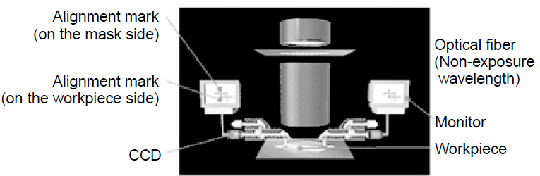
Procedure 2: Detection of Workpiece Alignment Mark
Procedure 2 is the method for detecting the workpiece alignment mark. A s the light used to illuminate the workpiece alignment mark, a non -exposure wavelength light is introduced from the alignment microscope via a halogen fiber. This allows independent detection of the workpiece alignment mark regardless of the mask alignment mark. After detection of the workpiece alignment mark, the workpiece is moved for alignment. The relative positions of the mask and the alignment microscope do not change within a short period of time. Therefore, the on -axis TTL allows alignment with the non-exposure wavelength. This is the alignment method proposed by USHIO.
1-3. Auto Scale Function
On the printed -circuit board, expansion/contraction of the pattern varies greatly depending on the process. From experience, the maximum expansion/contractio n amount ranges from 250 to 500 PPM. Variance of the expansion/contraction amount may reach approx. 100 PPM within the same lot. The actual expansion/contraction amount of the board varies depending on the individual board characteristics. Thus, it is diff icult for the mask correction method to achieve a high overlay accuracy.
The auto scale function of USHIOユs system allows expansion or contraction of the mask image projected on a workpiece by changing the projection magnification. The projection magnifica tion is determined by measuring the actual pitch of the workpiece alignment mark.
1-4. Throughput
The system throughput varies depending on the alignment mode selected during the exposure process. USHIO's system allows any of the following three alignment modes to be selected:
- (1) Die-by-die
This allows direct alignment of the mask alignment mark and workpiece alignment mark during each exposure run. - (2) Quasi die-by-die
This allows direct alignment of the mask alignment mark and workpiece alignment mark during exposure of the first shot of each workpiece. In this case, the exposure process is performed on assumption that the relative positions of the mask and alignment microscope do not change. - (3) Global
This mode estimates the designed exposure position from the reference marks on the workpiece and performs exposure of each shot.
Among the above three alignment modes, the quasi die-by-die mode is the most practical alignment mode, The throughput of the system operating in this mode can be calculated by the following formula: Process time per layer = (Alignment time + Exposure time) x Number of shots + Time required for workpiece replacement.
Where the alignment time and the time required for workpiece replacement are approximately 1.5 seconds and 10 seconds, respectively.
2. EFFECTIVENESS DURING PROCESSING OF ACTUAL BOARDS
2-1. Expansion/Contraction of Printed-Circuit Boards
The expansion/contraction of an actual printed-circuit board varies depending on the base material, machined patterns, process conditions, and other factors. USHIO's system allows measurement of the expansion/contraction amount of the actual board during exposure process. Either two or four measuring points can be selected at determination of the system specifications. For a normal p rinted-circuit board, the expansion/contraction amount differs between the horizontal (X) and vertical (Y) directions. Therefore, it is desirable that the projection magnification is determined by measuring the expansion/contraction amount in both the horizontal and vertical directions.
On the sample measured by USHIO, variance in the pitch was ±4 µm (3 s: 5.5 µm). Also, it can be proved that the expansion/contraction amount differs between boards and between shots within a board and that there is no systematic trend.
The size of the boards generally used ranges from 510 mm x 340 mm to 340 mm x 255 mm. Based on the above data, variance in the pitch may reach ±20 µm for 500 mm. This is the data obtained during processing of samples; variance in the expansion/contraction amount during processing of an actual workpiece may become further greater.
From such behavior as above during expansion/contraction, it becomes impossible to handle expansion/contraction of the board with the conventional mask correction method. For example, if an overlay accuracy of ±25 µm is required, it can be considered to deteriorate the product yield.
2-2. Advantage of Auto Scale Function during Overlay Exposure
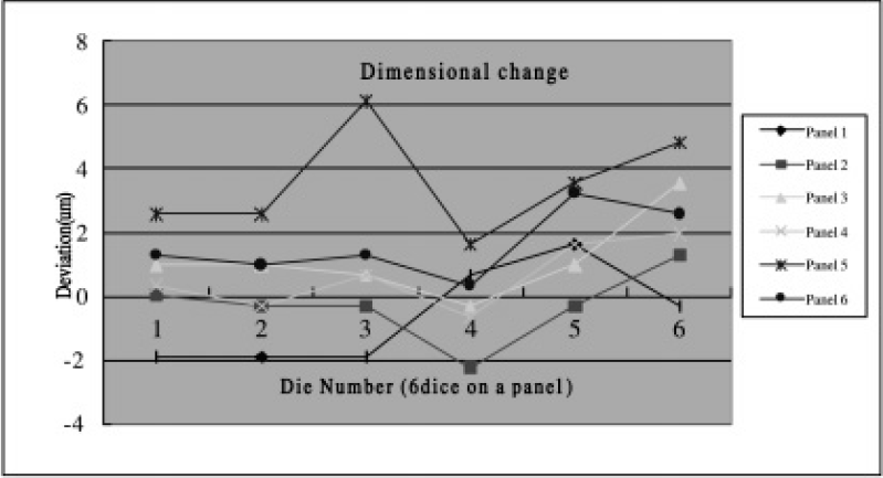
The following shows a pattern shift measured at the alignment mark after exposure of a sample board. The sample board is 510 mm x 340 mm, and 6 shots of exposure are performed at two rows by three columns. As the process recipe for exposure, the alignment tolerance is ±1 µm in the X/Y direction and the pitch tolerance is ±1 µm. The pitch tolerance is used to correct the mask size with the auto scale function.
Evaluation performed by USHIO has proved that the overlay accuracy of approx. ±5 µm can be achieved by optimizing the exposure area. The evaluation result at USHIO is introduced as follows:
Number of samples: 90 shots
Measuring instrument: Mitsutoyo Quick Vision (QV606 Super)
Measurement repeatability: ±1 µm
The variances at the alignment mark estimated from the log data obtained during exposure process were 2.3 through 2.6 µm (3 σ). The measurement results of the actual workpieces include variance of the measurement repeatability and variance of each alignment mark. Therefore, it can be considered that these results are greater than the variances estimated from the log data.
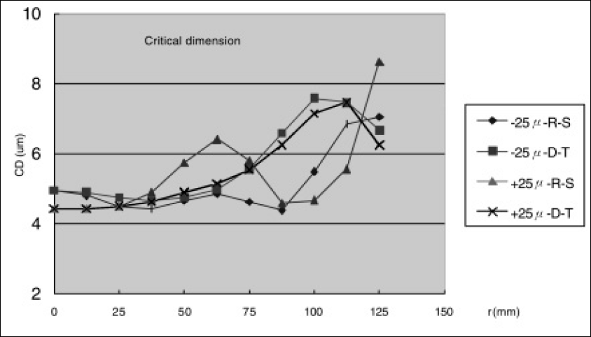
2-3. The critical dimension
Among the exposure performance , the critical dimension (CD) of the pattern play an important role for the yield. CD is essential performance of PWB manufacturing . In additionto the exposure lens performance, CD is influenced by the resist performance and development condition . We have evaluated due to dry-film resist. Effective exposure area is 250mm diameter.
Resist type : RY-3210EA Hitachi kasei
Resist thickness : 15um
Exposure energy : 110mJ/cm2 at 365nm
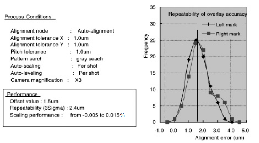
Repeatability of overlay accuracy
3. ROAD MAP FOR FUTURE DEVELOPMENT OF EXPOSURE SYSTEM
According to the road map of SIA published in 1999, the FBGA/CSP and flip-chip boards will require resolution of 50 µmL/S and 20 µmL/S, respectively, in 2002. We at USHIO plan to release exposure systems that mount the projection lens with the effective diameter of Φ250 mm and the resolution of 12 µmL/S in 2001, and those that mount the projection lens with the effective diameter of Φ200 mm and the resolution of 5 µmL/S in 2002. In addition, we are planning to develop the alignment mechanism and other components that allow further high-speed processing.
4. SUMMARY
We at USHIO marketed a step-and-repeat projection exposure system for printed-circuit boards in April 1999. This system features an exposure process with no contact between a workpiece and the mask, high alignment accuracy achieved by utilizing TTL on-axis alignment using a non-exposure wavelength, and provision of the auto scale function.
In particular, enhancement of the overlay accuracy and non-contact exposure process allows achievement of a high yield. In addition, enhancement of exposure accuracy allows an increase in the margin of the process other than exposure. It can be expected that the demand for the boards mounted with flip-chip devices will increase. In such a technological trend as above, the step-and-repeat projection exposure technology will become indispensable.