光技術情報誌「ライトエッジ」No.22(2001年9月発行)
IPC Printed Circuits Expo 2001技術フォーラム
Presented at IPC Printed Circuits EXPO® 2001
www.ipcprintedcircuitexpo.org
(2001年4月)
High Overlay Accuracy Using Scaling Method in PWB Photolithography
Toshiyuki Matsuki and Yoneta Tanaka
USHIO Inc.
Aoba-Ku, Yokohama, Japan
Abstract
There are three typical challenges in manufacturing printed circuit boards (PCBs): enhancement of the overlay accuracy of the exposure pattern, decrease in the fine pattern size and enhancement of the product yield. To meet these challenges, the step-and-repeat projection exposure method using a projection lens is effective. As its most prominent feature, the step-and-repeat projection exposure method allows non-contact patterning. It can also measure the expansion/contraction ratio of the actual pattern at each shot so as to allow projection of the mask at the corresponding expansion/contraction ratio.
It can be considered as essential in the future to introduce the step-and-repeat projection exposure system into production of the interposer boards for BGAs/CSPs, which are expected to increase in production volume, and the PCBs for digital equipment.
This paper will report basic studies of a step-and-repeat projection exposure system and its actual machine performance.
Introduction
In recent years, high resolution and high overlay accuracy have been required for PCBs such as MPU packages. We developed a step-and-repeat projection exposure system for PCBs, aiming to achieve the high resolution, high overlay accuracy and enhancement of the product yield.
Circumstances at when the step-and-repeat projection exposure method becomes effective is for products that require an overlay accuracy of ±30 m and a minimum line width of less than 50 m. In addition, this method is effective for cases in which a mask defect has caused a series of defects.
A PCB expands or contracts asymmetrically during production. The conventional system has reduced deterioration in the overlay accuracy by correcting the mask. However, because the expansion/contraction amount varies in different areas within the same board, the conventional system has a limit in enhancement of the overlay accuracy and yield. Therefore, it can be considered that the use of the step-and-repeat projection exposure method and the auto scale function is essential for exposurein PCBs at high accuracy.
The application of the step-and-repeat projection exposure system to the future manufacturing of PCBs is an important topics.
Basic System Performance
Projection Lens and Resolution
The projection lens used for this exposure systems has an effective diameter of φ200 mm; projection lens with the effective diameter of φ50 mm are also available for high-resolution systems. In addition, a high-resolution projection lens with effective diameter of φ200 mm is under development. The specifications of these lens are shown in Table 1.
As resolution samples of the process performed by the exposure system, Figure 1and Table 2 shows SEM photographs of three photoresist types processed by the projection exposure method.
Because of the projection lens is telecentric type. the exposure system has a long depth of focus.
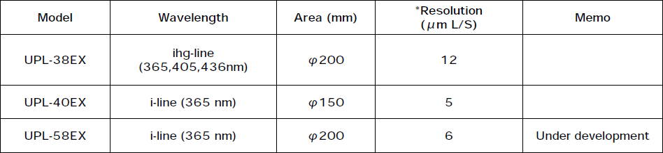
Table 1 - Lens List
* Based on USHIO's Evaluation standard
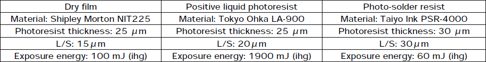
Table 2 - Exposure Methods and Resist Types
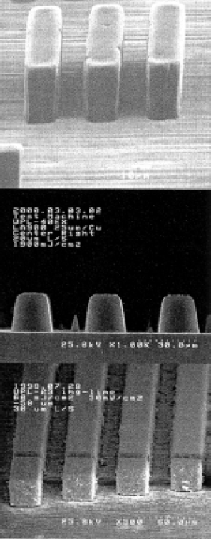
Figure 1 SEM Images of Photoresists Processed by Projection Exposure
Auto Scale Function
On the PCB, expansion/contraction of the pattern varies greatly depending on the process. From experience, the maximum expansion/contraction amount ranges from 250 to 500 PPM. Variance of the expansion/contraction amount may reach up to 100 PPM within the same lot. The actual expansion/ contraction amount of the board varies depending on the individual board characteristics.
Especially variance of the expansion/contraction on one panel is fatal for the mass production. Thus, it is difficult for the mask correction method to achieve high overlay accuracy.
The auto scale function of the system allows expansion or contraction of the mask image projected on a work piece by changing the projection magnification. The projection magnification is determined by measuring the actual pitch of the workpiece alignment mark in each panel or each shot.
The expansion/contraction of an actual PCB varies depending on the base material, machined patterns, process conditions and other factors. the system allows measurement of the expansion/contraction amount of the actual board during exposure process. Either two or four measuring points can be selected at determination of the system specifications. For a normal PCB, the expansion/contraction amount differs between the horizontal (X) and vertical (Y) directions. Therefore, it is desirable that the projection magnification is determined by measuring the expansion/contraction amount in both the horizontal and vertical directions.
The size of the boards generally used ranges from 510 mm x 340 mm to 340 mm x 255 mm. Based on the above data, variance in the pitch may reach ±20 µm for 500 mm. These data were obtained during processing of samples where variance in the expansion/contraction amount during processing of an actual workpiece may become further greater.
From such behavior as in the preceding, during expansion/contraction, it becomes impossible to handle expansion/contraction of the board with the conventional mask correction method. For example, if an overlay accuracy of ±25 µm is required, it can be considered to deteriorate the product yield.
Performance During Processing of Actual Boards
Long DOF During Resolution
On the PCB, thickness of the board varies depending on the process and the substrate.
From our experience, the maximum variance of thickness amount is 30µm on one board. To overcome the variance of thickness in each board, the auto-leveler function is effective; however thickness also varies within one actual board.
A exposure system with long DOF projection lens can make good profile patterns on the entire actual board with partial thickness variance.
The effectiveness of long DOF is shown in Figure 2. The DOF achieved a 100µm (± 50µm).
Uniformity of Critical Dimension
The pattern after development should not have only good shape but critical dimension for mask image. It scarcely needs to be said that the uniformity of critical dimension is an important factor.
Uniformity of critical dimension depends on optical performance (uniformity of UV intensity and resolution), development condition and photoresist characteristics.
The performance of critical dimension uniformity on actual board is shown in Figure 2. We selected dry-film resist; NIT215 Shipley Morton, for critical dimension evaluation. Critical dimension is measured by optical microscope. We evaluated critical dimension in ±50 µm focus conditions (100µm range) and in whole exposure area (φ200 mm) with the UPL-38EX lens.
The performance of critical dimension uniformity with different DFR is shown in Figure 3. Both DFR were processed under the same conditions at just focus with optimal energy, with UPL-38EX lens.
The pattern dimension located in the peripheral area is larger than the center. This variance depends on the distribution of projection lens resolution. As for next We expect the performance of critical dimension uniformity with new lens will achieve within ±1.5 µm for 100µm focus range.
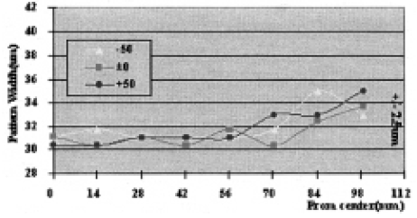
Figure 2 CD Uniformity vs. Focus (50mJ/cm2 )
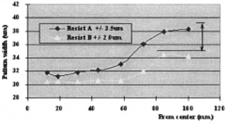
Figure 3 CD vs. Sigma (Focus: +/-0)
Advantage of Auto Scale Function during Overlay Registration
Figure 4 shows a pattern shift measured at the alignment mark after exposure of a sample board. The sample board is 510 mm x 340 mm, and six shots of exposure are performed at three rows by two lines. As the process recipe for exposure, the alignment tolerance is ±1 µm in the X/Y direction and the pitch tolerance is ±1 µm. The pitch tolerance is used to correct the mask size with the auto scale function.
Evaluation has proved that the overlay accuracy of approx. ±3 µm can be achieved by optimizing the exposure area. The evaluation result is introduced as follows:
Number of samples: 36 shots
Measuring instrument: Mitsutoyo Quick Vision (QV606 Super)
Measurement repeatability: ±1 µm
The variances at the alignment mark estimated from the log data obtained during exposure process were 2.3 through 2.6µm (3 σ ). The measurement results of the actual workpieces include variance of the measurement repeatability and variance of each alignment mark. Therefore, it can be considered that these results are greater than the variances estimated from the log data.

Figure 4 Pattern Shifts Following PC Exposure
RoadMap for Future Development of Exposure Systems
According to the roadmap of SIA, published in 1999, the FBGA/CSP and flip-chip boards will require resolution of 50-µ m L/S and 20-µ m L/S, respectively, in 2002. In 2001, we plan to release exposure systems that can mount a projection lens with effective diameter of φ 250 mm and the resolution of 12-µ m L/S. In 2002, we plan to introduce a system that can mount a projection lens with effective diameter of φ 200 mm and the resolution of 5-µm L/S. In addition, we are planning to develop the alignment mechanism and other components that allow further high-speed processing.
Summary
There have been step-and-repeat projection exposure systems for PCBs available since at least April 1999.
One system features an exposure process with no contact between a workpiece and the mask, high alignment accuracy achieved by utilizing TTL onaxis alignment using a non-exposure wavelength and provision of the auto scale function.
In particular, enhancement of the overlay accuracy and non-contact exposure process allowed achievement of high yield. In addition, enhancement of exposure accuracy allowed an increase in the margin of the process other than exposure. Industry expects that the demand for the boards mounted with flip-chip devices will increase. In such a technological trend, the step-and-repeat projection exposure technology will become indispensable.