光技術情報誌「ライトエッジ」No.24(2002年4月発行)
2001 International Conference on Solid State Devices and Matelials,
Extended Abstracts of the 2001 International Conference on Solid State Devices and Materials,Tokyo,2001,pp.182-183
(2001年9月)
A-5-3
Flash Lamp Anneal Technology for Effectively Activating Ion Implanted Si
T.Ito, T. Iinuma, A. Murakoshi, H. Akutsu, K. Suguro,T. Arikado, K. Okumura,
M. Yoshioka1, T. Owada1,Y. Imaoka2, H. Murayama2 and T. Kusuda2
Process and Manufacturing Engineering Center, Semiconductor Company, Toshiba Corp.
8 Shinsugita-cho, Isogo-ku, Yokohama 235-8522, Japan
Phone:+81-45-770-3662 Fax:+81-45-770-3577 E-mail: t-ito@amc.toshiba.co.jp
1Lamp Technology and Engineering Division, Ushio Inc.
1194, Sazuchi, Bessho-cho, Himeji, Hyogo 671-0224, Japan
2Development Department for Electronics Equipment, Dainippon Screen MFG. Co. Ltd.
322 Furukawa-cho, Hazukashi, Fushimi-ku, Kyoto 612-8486, Japan
1.Introduction
Device miniaturization requires reduction of the thermal budget in the annealing process for ultra-shallow junction and ultra-thin gate oxide. Recently, spike anneal technology has considerably reduced the time of the heating cycle. In heating the substrate above 1000°C, however, the total time of ramp-up and rampdown takes 10 sec or above.
In order to minimize the heating cycle, we newly developed a flash lamp anneal (FLA) technology. FLA was able to reduce the heating cycle within the millisecond range and was successfully applied to activation process by combining appropriate assist heating. In this paper, we first report fundamental results on electrical activation of impurities by using FLA technology.
2.Experimental
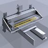
Figure 1 shows the fundamental configuration of FLA apparatus. This apparatus is composed of xenon flash lamps and tungsten halogen lamps for assist heating.
Figure 2 shows radiant spectrum of the xenon flash lamp and optical coefficient of Si. The radiant peak of the xenon flash lamp is in the range from 300 to 800 nm. Since the absorption edge of Si is approximately 1100 nm, Si sub strate can be effectively heated by the xenon flash lamp. The incident radiant energy density was measured with a calorimeter.
The sheet resistance of ion implanted (100)Si was measured as a function of the incident radiant energy density and the assist temperature. In these experiments, the substrates were irradiated for a short time in the range of 1-3 msec with the incident radiant energy density above several J/cm2.

Fig.1 fundamental configuration of FLA apparatus.
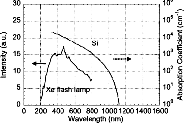
Fig. 2 Radiant spectrum of the xenon flash lamp and optical coefficient of Si.
3.Results and Discussion
FLA was applied to As implanted (100) Si substrates. The dose was 5 × 1015 cm-2 at 40 keV. The sheet resistance measured with a four point probe is shown in Figs. 3(a) and 3(b) as a function of the incident radiant energy density and the assist temperature.
It was found that the lower sheet resistance was obtained at the higher assist temperatures for the lower radiant energy density and for the higher radiant energy density at the lower assist temperatures. That is, the incident radiant energy density required for activation depends on the assist temperature. Slip generated at above 43 J/cm2 of radiant energy in the case of assist temperature of 400°C as shown in Fig. 3(a) due to the increase in thermal strain. On the other hand, Sheet resistance abruptly decreases with assist temperature. Therefore, the appropriate combination of the assist temperature and the radiant energy is neccessary for activating implanted impurities.
Figures 4(a) and 4(b) show SIMS depth profiles of B and As in (100)Si substrate after FLA, respectively. Implant conditions are 0.2 keV, 1 × 1015 cm-2 for B and 1 keV, 1 × 1015 cm-2 for As, respectively. Both show abrupt profiles with the high peak concentrations above 1021cm-3. This suggests that FLA technology has the possibility of creating the super-shallow junction below 20 nm under the optimum conditions.
Figure 5 shows SIMS depth profiles of In in (100)Si substrate before and after annealing. The implant condition is 150keV, 1 × 1013cm-2. The conventional furnace annealing and RTA resulted in decrease of the peak concentrations and considerable diffusion of the dopants with increasing temperature.
On the other hand, the profile for FLA is similar to that for the as-implanted case. Comparison of the sheet resistance and the electrical activation between the conventional annealing and FLA is summarized in Table I. After the conventional annealing, the sheet resistance was about 20 kΩ/□, and the elctrically active fraction was about 20 %. On the other hand, after FLA under the optimum conditions, the sheet resistance was 11.3 kΩ/ □, and the electrically active fraction was 76 %. That is, the maximum electrical activation for the minimum amount of diffusion can be obtained by FLA. From these results, it is considered that the annealing for longer time at higher temperature induces the deactivation of In.
It was found that the single shot was able to create an abrupt profile with higher activated In concentration as shown in Fig. 6. In the case that the number of flash shots was 2 and 3, however, the electrically active fraction was belonw 40 %. Thus, FLA is very effective in electrical activation of In maintaining as-implantd profile. This result is very useful for channel engineering in sub 0.1µm MOSFETs.
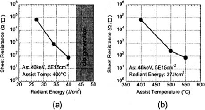
Fig.3 Sheet resistance of As implanted (100) Si substrate as a function of(a) the incident radiant energy density and (b) the assist temperature.
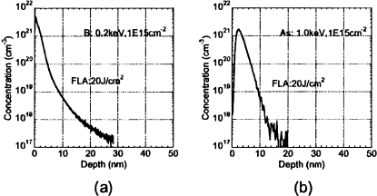
Fig.4 SIMS depth profiles of (a) B and (b) As in (100) Si substrate after FLA.
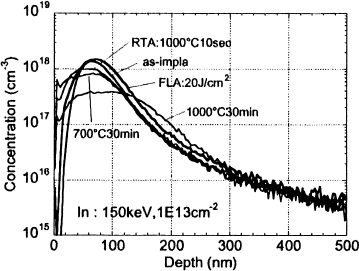
Fig.5 SIMS depth profiles of In in (100)Si substrate before and after annealing.
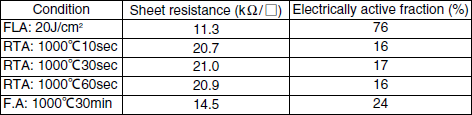
Table1 Measured characteristics of In implanted Si.
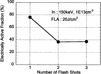
Fig.6 Electrical activation of In against number of flash shots,
4.Conclusion
FLA technology was applied to the electrical activation of ion implanted Si. An abrupt B, As and In profile with higher activated concentration was realized by using FLA. This result is due to extremely high rate ramp up and down thermal process. FLA will be one of key technologies in sub 0.1µm MOSFETs.