光技術情報誌「ライトエッジ」No.31(2008年10月)
ヨーロッパ太陽電池国際会議
(2007年9月)
FORMATION OF POLYCRYSTALLINE Si FILMS OVER 3 µm
IN THICKNESS ON QUARTZ SUBSTRATES
BY FLASH LAMP ANNEALING
Keisuke Ohdaira1, Yohei Endo1, Tomoko Fujiwara1, Shogo Nishizaki1, Kensuke Nishioka1, Hideki Matsumura1,
Takeshi Karasawa2, and Tetsuya Torikai2
1 Japan Advanced Institute of Science and Technology (JAIST),1-1 Asahidai, Nomi, Ishikawa 923-1292, Japan
2 R&D Center, Ushio Inc., 1194 Sazuchi, Bessho-cho, Himeji, Hyogo 671-0224, Japan
TEL : +81-761-51-1563, FAX : +81-761-51-1149, E-mail : ohdaira@jaist.ac.jp
ABSTRACT
Precursor amorphous silicon (a-Si) films of as thick as 4.5 µm in thickness formed on quartz glass substrates by catalytic chemical vapor deposition (Cat-CVD) are crystallized by flash lamp annealing (FLA). An inserted Cr film between the quartz substrate and the Si film acts to prevent peeling of the Si film. This poly-Si film reveals high crystallinity of approximately unity at the surface with high in-plane uniformity, whereas a-Si is remained in the vicinity of the Si/Cr interface. High-pressure water vapor annealing (HPWVA) is found to be effective for terminating defects in the poly-Si films generated during FLA. The poly-Si film after HPWVA shows a minority carrier lifetime of about 10 µs, indicating high feasibility of the poly-Si film to high-efficiency thin-film solar cells.
Keywords
Flash Lamp Annealing, Crystallization, Polycrystalline Si, Minority Carrier Lifetime, High-Pressure Water Vapor Annealing
1 INTRODUCTION
Formation of polycrystalline silicon (poly-Si) films of several µm in thickness on glass substrates and application of the poly-Si films to high-efficiency solar cells have been extensively studied [1-3]. This will lead to cost reduction of solar cells because of demanding less amount of Si and utilization of cheap glass substrates. In the case of crystallizing precursor amorphous Si (a-Si) by a conventional furnace annealing, at least several hours are needed for sufficient crystallization. Such a long process time seems to be a disadvantage for mass-production, and technologies for rapid crystallization of several µm-thick a-Si should be established.
The annealing time is an important factor for realizing such crystallization process. If the annealing time exceeds 1 s, the temperature of the glass substrate reaches approximately the same as that of the Si film of more than 700°C since the thermal diffusion length of a-Si and glass in 1 s is about 1 mm, resulting in thermal damage to the glass substrate. On the other hand, in the case of several nanosecond annealing, which has already been established in excimer laser annealing (ELA), only a surface of the µm-thick a-Si film is crystallized since thermal diffusion length of a-Si in 10 ns is less than 0.1 µm, indicating inadequacy of this process for crystallization of a µm-thick a-Si. For crystallization of the µm-thick a-Si without thermal damage to the glass substrate, millisecond annealing is appropriate because the thermal diffusion length of a-Si exceeds 10 µm and that of glass is suppressed within several tens of µm in 1-10 ms. Flash lamp annealing (FLA) is one of the technologies for realizing the millisecond treatment[4-6]. We have attempted to form device-quality poly-Si films on glass substrates and found that 1.5-µm-thick a-Si films on quartz substrates can be crystallized by FLA and the poly-Si films show minority carrier lifetimes of more than 5 µs after high-pressure water vapor annealing (HPWVA) for defect termination[7,8]
In this study, we have succeeded at crystallizing 4.5-µm-thick precursor a-Si on chromium (Cr) -coated quartz substrates by FLA. Fundamental properties of the poly-Si films have also been investigated in order to clarify feasibility of the high-efficiency thin-film solar cell using the poly-Si films.
2 EXPERIMENTAL
Figure 1 shows a schematic diagram of the sample structure. Instead of low-cost glass substrates, 20 × 20 × 0.7 mm quartz substrates were used for fundamental research. Cr films of 60 or 200 nm in thickness were first formed on the quartz substrates by sputtering, followed by preparation of a-Si films of 4.5 µm in thickness by catalytic chemical vapor deposition (Cat-CVD). The a-Si films show a hydrogen content of as low as approximately 3%, which is suitable for such rapid crystallization processes having an issue of hydrogen bubbling during annealing and resulting peeling of the Si films.
For crystallization of the a-Si films, we used FLA with a millisecond-order duration. Only one pulse was irradiated for one crystallization process. No dehydrogenation process was performed to precursor a-Si films before FLA. The pulse duration was fixed throughout this study, whereas lamp irradiances were systematically changed to find proper annealing condition.
Crystallization of the Si films and the crystallinity were characterized by Raman spectroscopy using He-Ne laser. Minority carrier lifetime was measured by microwave photoconductivity decay (µ-PCD) with a pulse laser of 349 nm in wavelength for generating excess carriers. High-pressure water vapor annealing (HPWVA) was performed to some of the poly-Si films at 300-500°C under a pressure of about 1 MPa for 1 h.
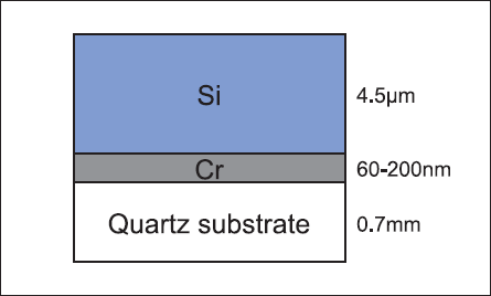
Fig.1 : Schematic diagram of the sample structure.
3 RESULTS AND DISCUSSION
Figures 2(a)-(d) show surface photographs of the Si films after FLA. As shown in Fig. 2(a), serious peeling or ablation of the Si film occurs during FLA in the case without Cr insertion. There is no process window for crystallization of the whole area of the 20 × 20 mm Si film deposited directly on the quartz substrate. In the case with insertion of the Cr film, crystallization of the a-Si occurs without peeling of the Si film as shown in Figs 2(b) and (c) although peeling of the Si films occurs in too much lamp irradiance. The whole area of the a-Si film is crystallized under an optimized lamp irradiance as shown in Fig. 2(c). These results clearly indicate that the Cr film acts effectively to improve adhesiveness of Si film. Thermal distribution in the Si film during FLA, which is caused by heating of the Si film edge and nonuniform thermal diffusion from the Si film into the glass substrate due to less amount of glass material below the Si edge, may also be relaxed by the Cr film having much larger thermal conductivity than glass and Si, resulting in suppression of peeling of the Si film from the edge region. As shown typically in Fig. 2(b), Crystallization tends to occur mainly from the edge of the Si film towards inside, which is probably due to additional heating of the Si film edge. This crystallization is not due to metal-induced one because the same crystallization occurs even when a silicon nitride (SiNx) film is inserted between the Si and Cr films.
Figure 3 shows Raman spectra of the 4.5-µm-thick poly-Si film measured at the surface and Si/Cr interface after wet chemical etching. At the Si surface, a clear c-Si peak is observed, whereas no a-Si peak is seen, indicating formation of poly-Si with high crystallinity of approximately unity. Almost the same spectra are observed from the whole surface, which indicates high in-plane uniformity of crystallization. The full width at half maximum (FWHM) of the c-Si peak is about 8 cm-1, larger than that of the monocrystalline Si of 4 cm-1. This result indicates that the poly-Si film consists of small crystal grains of several tens of nm or less[9]. The peak originating from a-Si centered at 480 cm-1 is also seen in the spectrum measured at Si/Cr interface. This reveals that a-Si is not completely crystallized at Si/Cr interface, which may be caused by a rapid thermal diffusion into the Cr film during FLA. This remained a-Si might act effectively to prevent from peeling of the Si film.
Figure 4 shows a decay curve of microwave reflection from the poly-Si after HPWVA under the optimized temperature of 350°C. Two decay components are clearly seen. We consider the first rapid decay as the recombination and the second slow decay with the order of several hundreds of ps as the safety trap effect caused by shallow energy levels[10-11] starting to act due to effective passivation of deep levels by HPWVA. The shallow trap levels may not deteriorate solar cell properties since such levels are probably filled constantly with carriers during actual operation with continuous irradiation of sunlight. The recombination lifetime is estimated to be approximately 10 µs, indicating excellent crystal quality and high feasibility of high-efficiency thin-film solar cells using this poly-Si. Such a long recombination lifetime cannot be observed without HPWVA, showing necessity of effective defect termination processes for using this poly-Si film to solar cells and significant effect of HPWVA to the poly-Si film.
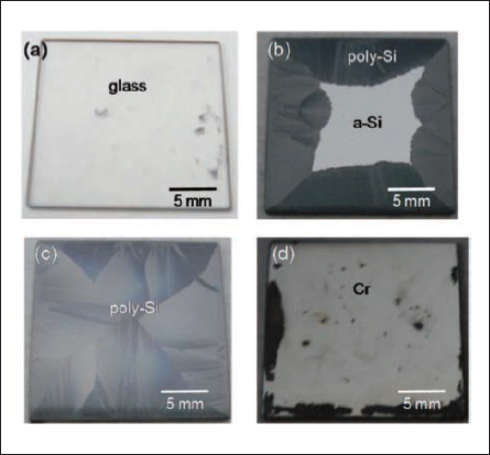
Fig.2: Surface photographs of Si films after FLA;
(a) without insertion of the Cr film,
(b) with insertion of the Cr film annealed under low lamp irradiance,
(c) under proper lamp irradiance,
(d) under high lamp irradiance.
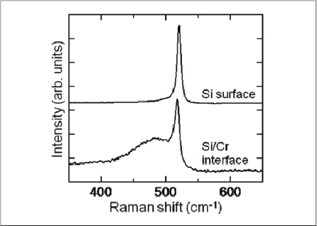
Fig.3 : Raman spectra from Si films after FLA measured at the surface and Si/Cr interface.
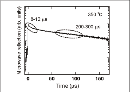
Fig.4 : Decay curve of microwave reflection from 4.5-mm-thick poly-Si formed by FLA after HPWVA at 350°C.
4 CONCLUSIONS
Precursor a-Si films of as thick as 4.5 µm in thickness formed on quartz glass substrates by Cat-CVD method are crystallized by FLA without peeling of the Si. The inserted Cr film between the quartz substrate and the Si film, which can also be utilized as a back electrode and a back reflector in an actual solar cell structure, acts to prevent peeling of the Si film. The poly-Si reveals high crystallinity at the surface with high in-plane uniformity, whereas a-Si is remained in the vicinity of the Si/Cr interface. HPWVA is effective for terminating defects and the poly-Si film after HPWVA shows a minority carrier lifetime of about 10 µs, indicating high feasibility of this poly-Si film to high-efficiency thin-film solar cells.
ACKNOWLEDGMENTS
This work is supported by the NEDO (New Energy and Industrial Technology Development Organization) project of R&D for next-generation PV systems.