光技術情報誌「ライトエッジ」No.41(2014年12月発行)
大学研究室を訪ねて Campus Lab㉖
光と有機材料を利用した
「ユビキタスセンシング技術」の開発
九州大学大学院システム情報科学研究院 I&E ビジョナリー特別部門
教授 興 雄司 先生
九大百年、躍進百大、新たな百年を目指して
―九州大学
九州大学は、11の学部をはじめ、17の学府と16の研究院を置いた大学院、特色ある付置研究所、専門職大学院で構成され、西日本を代表する基幹総合大学である。
その母体は、1903年に京都帝国大学の分科大学として福岡に開設された、附属医院をもつ福岡医科大学である。1911年、この福岡医科大学と新設の工科大学が統合した九州帝国大学が創設され、1919年に医科大学は医学部に、工科大学は工学部となり、同時に農学部が開設された。その後も法文学部や理学部の新設、高等学校や専門学校の合併を経て、1949年に新制の国立九州大学となった。
九州大学は、その後も時代の要請に呼応し、学部の改組・新設・増設、他大学との統合などを推進し、“アジアに開かれた「知」の世界的拠点”と呼ぶにふさわしい規模と陣容を備え、広く社会に貢献し続けている。
九州大学は、その「教育憲章」や「学術憲章」に示されているように、教育においては、世界の人々から支持される高等教育を推進し、世界において指導的な役割を担い活躍する人材を輩出し、世界の発展に貢献することを目指している。また、学術研究においては、人類が長きにわたって遂行してきた真理の探究と、そこに結実した人間的叡智を尊び、これを将来に伝えていくとともに、新しい展望を開き、世界に誇り得る先進的な知的成果を生み出していくことを使命としている。
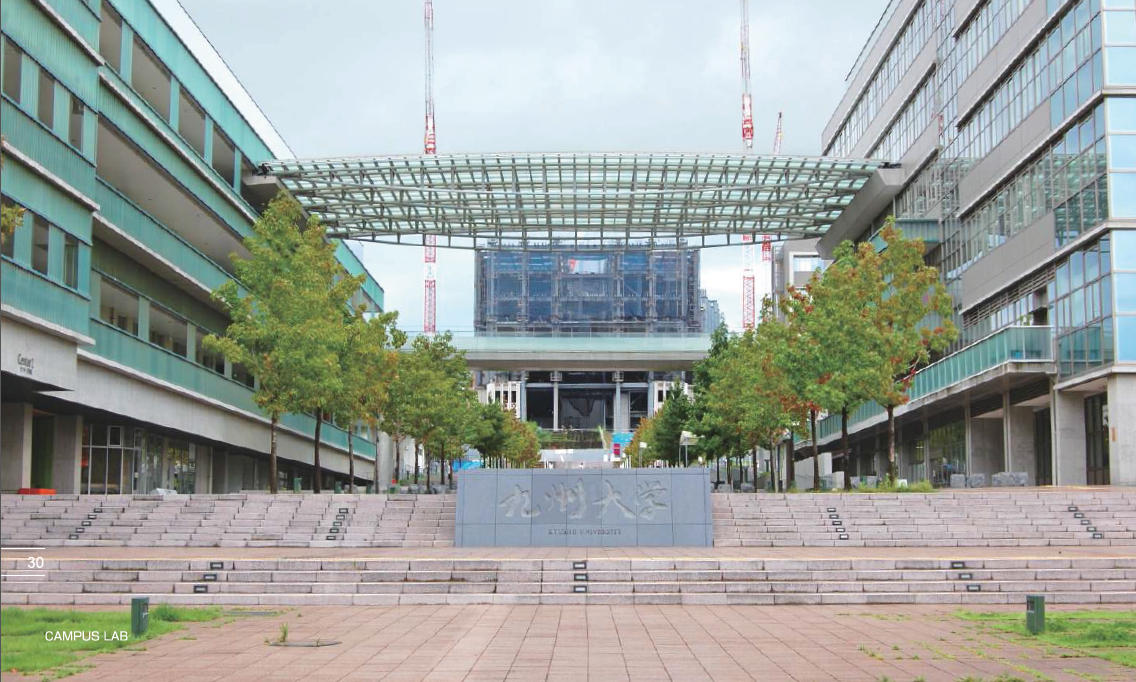
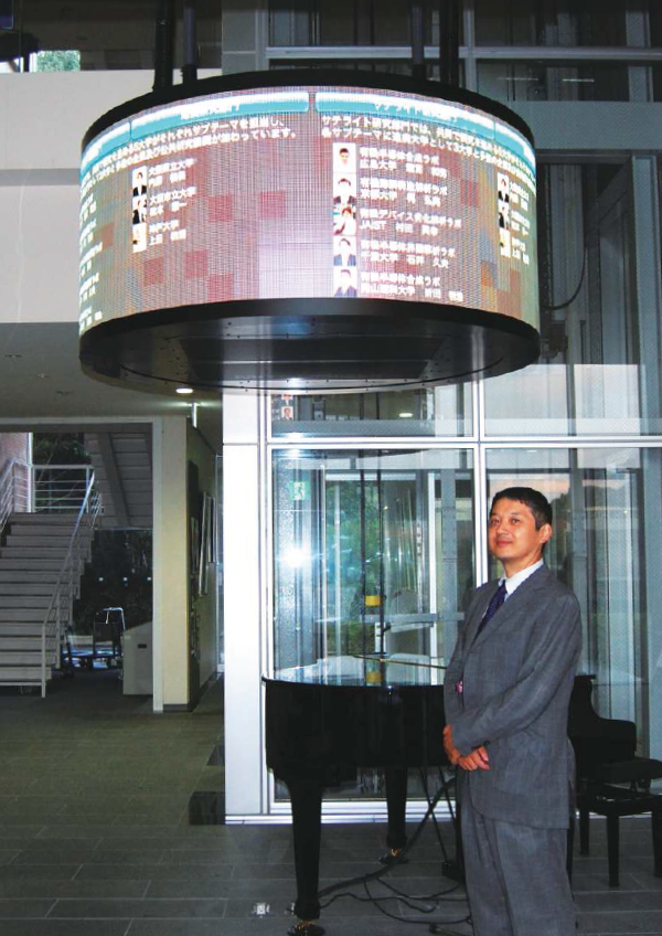
▼九州大学 伊都キャンパス: 伊都キャンパスは敷地面積275ha(福岡ヤフオク!ドーム 約40個分)で、九州大学最大のキャンパスである。 ここでは、全学部の1年生と工学系学部生、そして工学系、社会科学系、数理学の大学院生が学ぶ。基礎・基盤的研究はもとより、大型の先端的研究、産学官連携による取組みや次代を担う人材養成プログラムなど、社会のさまざまな課題に対応する教育研究活動を展開している。現在、センター1号館を新設中(写真中央)。
世界から伊都キャンパスへ
―人々を結ぶ架け橋
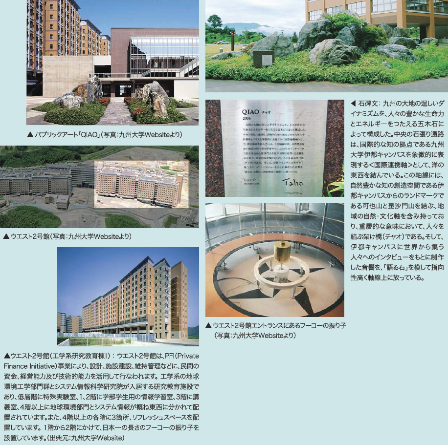
ウエスト2号館を背にした総合学習プラザの前にあるパブリックアート「QIAO」。世界的アーチストたほりつこ氏の作品である。一見、造園のように見えるが、石や草花をモチーフに、住民との綿密な共同作業を通して、地域の活性化を象徴しているという。
氏の作品には、世界を舞台に「多文化宣言」(1997)や「夢シャワー」(1999)、「インディゴ キルト プロジェクト」(2003)など多数ある。「たほのパブリックアートが、多文化間の軋轢という社会的にシビアな問題を扱っていながら、一方ではすがすがしい感触をもっているのは、夢、詩、瞑想といった要素をそこに導入して、個々人の精神の豊かな広がりを公共空間に生じさせる可能性を感じさせるからだ」(倉林 靖/美術評論家)とあるように、氏の作品は、パブリックアートと呼ぶにふさわしく、社会に向けた重要な示唆と提言を感じさせる。このことが九州大学の「教育憲章」や「学術憲章」に相通じるものがあるのかもしれない。
未来社会を支える
システム情報科学の展開
システム情報科学府・研究院が掲げる基本理念である「情報科学(I)と電気電子工学(E)の融合による学問体系の創出と社会貢献」のもとに、学問体系の基盤分野で世界最先端の研究・教育を加速する「不易」体制の強化社会要請に応え、新しい研究領域を絶えず創成・展開する「流行」体制の創出の相反要請を可能とすることを目指して、九州大学が戦略的に推進する大学改革活性化制度のもとに、2012年度、既存部門から独立した「I&Eビジョナリー特別部門」が新設された。
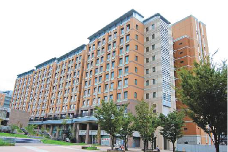
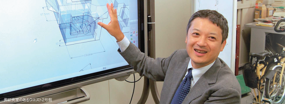
▲ 興研究室のあるウエスト2号館
I&E ビジョナリー特別部門の研究領域
I&E ユビキタスセンシンググループ
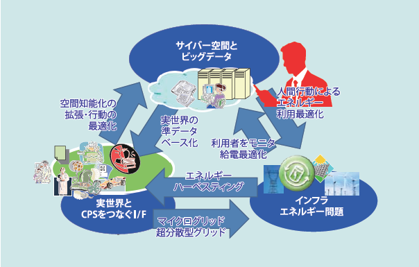
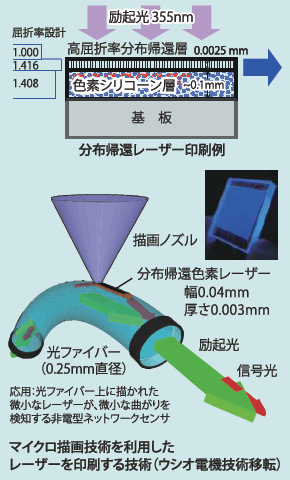
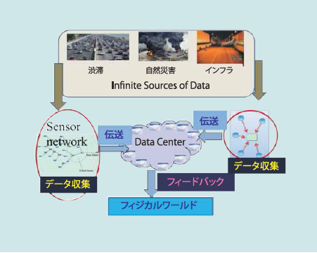
CPSによる持続可能なIT社会の発展(下図)に向けて、このグループでは、光センシングを軸とした光エネルギーハーベストによる無給電センサーや、諸情報の光学情報への変換を可能とする光センシングデバイスの研究を行っている。実世界の膨大な情報を、エネルギーの消費を増大させずにサイバースペースへのビッグデータへと反映させるという、実世界への超分散型インターフェースの構築を目指している。
研究では、有機材料のデバイス応用とレーザー工学が中心となっている。図1は固体中を分子が高速移動するPDMS材料を活用した青色レーザー構造の開発例、図2はインクジェットによる有機マイクロディスク構造の作製例である。リソグラフィーの1/100以下の時間とコストで、センサーの作製が可能としている。
▲ 図1
▲ 図2
I&E LSIシステムグループ
このグループでは、半導体が産み出すビッグデータ・CPSの実現(図1)を目指している。具体的には、図2に示すように、データを継続的に収集するためのバッテリーレスセンサノード、収集した膨大なデータをデータセンターまでに伝送する超高速(10GBPSを超える)の無線システムの研究開発を行っている。
▲ 図1 半導体が産み出すビッグデータ・CPS
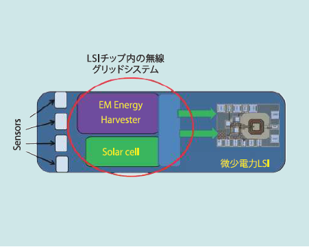
▲ 図2 バッテリーレスセンサノード
I&E ワイヤレスデバイスグループ
このグループでは、ビッグデータを利活用するために必要なネットワークデバイスの開発を行っている。さまざまな機器を無線ネットワークでつなぎ、機器同士が情報をやりとりすることができれば、これらが協調して、常に最適な制御を行うことが可能となり、IとEの融合が達成できる。
直近において、UHF、携帯、及びGPSの電波に対応したM2M (Machine to Machine、機器間通信)用通信モジュールを開発。これによって、無線通信用ICの高効率化設計と、実装方法の両面からアプローチすることで、機器の高効率化を実現した。
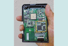
▲ M2M用通信モジュール
I&E 新材料・デバイスグループ
新しい材料の発見は、科学技術のブレークスルーを生み出し、産業さらには社会に大きなインパクトを与える。このグループでは、コンビナトリアル法という超高速材料探索技術を用い、革新的光・電子デバイスを実現する新規半導体材料やレアメタル代替材料の探索研究を行っている。
また、新材料を用いた全く新しい超高速・超低消費電力信号処理デバイスや、量子効果を利用した超高効率太陽電池の開発を通じて、資源・環境・エネルギーといった現代の技術課題にも挑戦している。
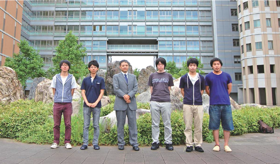
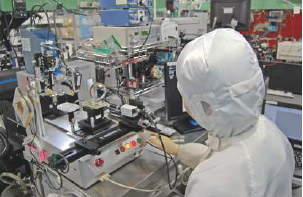
▲研究室の皆さん(左から3人目が興先生)
▲ミクロンサイズのポリマーワイヤーの架橋のようす: 直径5µm、長さ30µm、位置安定性は30nm程度
※ウシオと共同研究 ※ホルダーは3Dプリンタにより制作
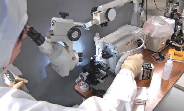
▲細胞試料のスライス技術を応用したレーザー出力面を作成
▲ 九州大学大学院 国際博士課程教育リーディングプログラム: 高精度3DCAD、3Dプリンタ、i-Pad等を設置し、実際に分子のモデルを作ったり、デバイスのモデルをつくるなどして研究分野の異なる学生同士のブレーンストーミングを推進している。IT関係の設置、プログラムの構想には興先生も大きく貢献している。
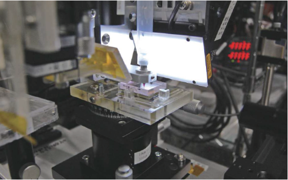
▲マイクロディスペンス法による3次元描画
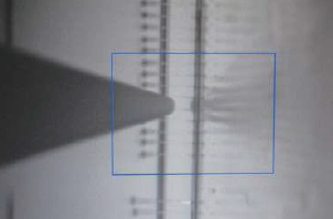
▲ミクロンサイズのポリマーワイヤーの架橋のようす顕微鏡拡大図
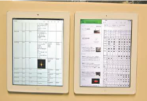
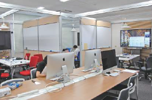
▲タブレットを利用したペーパーレスな情報共有システム: 各研究者のデータが一括管理されており、PCとも無線でデータが共有できている。
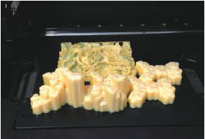
▲3Dプリンタで制作されたサンプル
▲全てのパネルに有機ELが採用されているディスプレイ
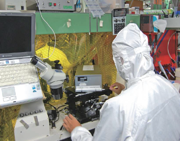
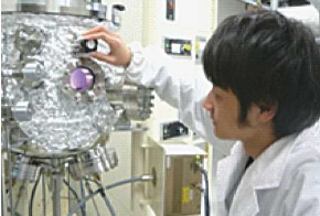
▲ エキシマランプによる表面改質および深紫外露光装置 ※エキシマランプはウシオ製

▲研究に非常に有用な3Dプリンタ
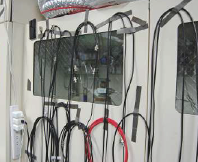
▲世界最強のネオジウム磁石を利用した配線管理:
強力な磁石を採用することで、わずらわしい配線の管理を着脱可能なスタイルに変更してある。新しいもの、ユニークなものを実際に触って確かめたいという興教授ならではの発想による。
「興先生に聞く」
蓄積したデータを確認することで時間を巻き戻す
人に役立つ科学技術を
- Q1:先生がユビキタスセンシング技術の開発を行なうきっかけは何でしょう?
- A1:まず、科学技術は「人の役に立ってナンボ」だと思っています。
私は、学生時代、日本で初めて色素レーザーの研究をされていた前田先生のもとで研究していました。この時代から、人々の生活が世界レベルでどんどん向上していきましたが、それが成り立ってきたのは、全て、技術の向上があるからだと思っていました。学生時代にレーザーの研究をしていた時も、環境に興味があって、エキシマレーザーを使ってオゾン層の破壊状況やオゾンホールの測定にチャレンジしていました。
最近は技術が進化しすぎて、オーバーテクノロジー気味になって、そのため、パーソナルユースなものが脚光を浴びてきていると感じています。例えばスマホのように、最高クラスのスペックではなくても個人で持てる完成度の高いものなどです。 昔は、先端技術が産業を引っ張っていたと思いますが、今は、人にマッチする技術が求められてきているのではないでしょうか。そういう人にマッチしたモノ作りがしたいという思いが、きっかけといえるかもしれませんね。
見えないもの
- Q2:先生のご研究は社会にどのような影響を与えていくのでしょうか?
- A2:人が見えないものを見えるように、例えば、紫外線、赤外線、化学物質、室内の塗装物質からの臭い、過去の温度などを可視化するというイメージですね。それによって危険を事前に察知したり、蓄積したデータを確認することで過去に戻れたりします。つまり、時間を巻き戻すことができると考えています。
回り道をする
- Q3:ご研究にはいろんな困難があったと思いますが、ご苦労されたことはどんなことでしょう?
- A3:苦労だとは言い切れませんが、回り道が多いことでしょうか。
例えば、人に聞いたら分かることも、あえてすぐに聞いたりしないようにしています。というのも、ムダだと思われていることでも、自分で1度やってみて、自分の意見を持つまでやれば、これらの経験や情報があとできっと役に立つと思っているからです。
あらゆることに興味を
- Q4:先生がご研究をするうえで、大事にされていることは何でしょう?
- A4:「あらゆることに興味を示す努力をすること」ですね。
ものごとを全て自分で考え、見解をもつ。これは、自分の意見を持つまで、限界まで考えたうえで、人の意見を聞き、尊重するということです。私は、どちらかというとあまり本を読んだり、人に聞いたりするタイプではなく、自分で考えるタイプだと思っています。
ウシオにしかないモノ作りを
- Q5:ウシオとの共同開発を進めていくうえで、ウシオに求めることは?
- A5:挑戦者であり続けてほしいと思います。
私は、ウシオさんは新規開拓を大事にされている会社で、特に、産学連携のコミュニティーを積極的に進めている会社だと思います。半導体産業のように、コロコロと変化する産業もありますが、ウシオさんにしかないモノ作りの技術を、ぜひ大事にしていってほしいですね。
回り道を恐れないで
- Q6:最後に、若い人に伝えたいことをお聞かせください。
- A6:「回り道を決して恐れないで」と言いたいですね。
回り道はムダではありません。若い間はどんどん吸収することができます。特に、失敗や回り道から学ぶことは多く、これらは本やインターネットからは学ぶことのできない、他の人が経験することのできない自分だけの経験です。それがあとで身になり、将来の役に立ちます。
私は、年を取った時にどれだけの回り道をしたかが糧になると思っています。ぜひ回り道や失敗を恐れず、挑戦する心を忘れないでほしいですね。
光と有機材料を利用した「ユビキタスセンシング技術」の開発
CAMPUS LAB 26 大学研究室を訪ねて
主な研究発表 第61回 応用物理学会春季学術講演会 講演予稿集 (2014 春 青山学院大学)
Bits-Oriented を目指した
モノリシックPDMS 光学システム設計
PDMS monolithic optical system design as “Bit Oriented Optical Fabrication”
九州大学1 ・ ウシオ電機2 ○楊 帆1, 森田 金市2, 吉岡宏晃1, 興 雄司1
Kyushu Univ.1, Ushio.2 ○Fan Yang, Kinichi Morita, Hiroaki Yoshioka, Yuji Oki
E-mail: oki@ed.kyushu-u.ac.jp
3Dプリンターが昨今注目を浴びている。MITのNeil Gershefeld が“How to Make Almost Anything”を発表してbits and atoms という概念に基づく新しい物作りを提唱して1)以来、コンピューター情報(=bits)に容易に対応しうる各種加工機の最後に登場した3D printer は、もっとも bitsに実際の物(atoms)を半自動構築させる術に優れ、Bits-oriented な物作りを身近な物とした。こうした物の有り様をbits に落とし込むBits-oriented な物作りでは、bits のネットワーク透過性と、改良・改善の容易さが享受でき、新しい人々のアイディアの結集・相互扶助・相互作用が進みつつある。我々は、こうしたパラダイムを光学システムへも拡張すべく、単一材料の空間配置のみで光学システムを実現する研究を開始した。
単一材料=monolithic から多様な展開が期待できる光学システムを創造する過程において、我々はアプリケーションや基本光学システム・補助エレクトロニクスには既存プラットフォームを活用することを考え、その候補として汎用タブレットに着目した。これに組みあわせてモノリシック且つmm〜cm サイズの光学システムを構築するにはガラス密着性の高いポリジメチルシロキサン(PDMS)が適している。PDMS はUV 透過性が高く、接着によるガラスとの安定した光結合、容易な剥離を提供するため、タブレット液晶から光を取り込み、内部で光学処理を行い、タブレットカメラに光学出力を結合するという一連の光学システム処理を安定して提供できる。
Fig.1 に示す様なPDMS をマトリクスとする光学システムを実現するには、(1)高い減光性の遮光壁・光トラップ、(2)集光構造 (3)波長フィルターなどを自在に配置することがまず必要になる。PDMS は固化後の追加工が困難であるため、3Dプリンター(Agilista-3000, Keyence)で出力した最適設計済みのアクリル型からPDMS を重合転写して施した。(1)については使用した高精度PDMS(SIM-360, 信越化学)にカーボンブラックコンパウンドを分散させ、導光PDMS層や吸光PDMS 層を埋没・接合させることにより遮光壁を構築した。この反射防止遮光壁では、短い吸収長(14µm)と、低い境界反射散乱率10-3 が実現できている。これにより外部からの光雑音や多重散乱による迷光を低減でき、システム全体の小型化が可能となった。(2)では球面型の埋め込みによるレンズ様面を配置した。(3)についてはSudan 色素の乾式含浸分散による532nm 吸収PDMS フィルターによりOD5 を得た。
今回、PDMS ベースでその成型を基準とした光学システム要素技術開発を行った。今後、これを組みあわせてタブレットと融合した光学システムを試作していく。
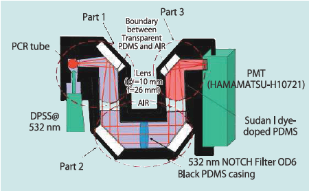
Fig.1 作製したPDMS LIF 検出器の例
光と有機材料を利用した「ユビキタスセンシング技術」の開発
CAMPUS LAB 26 大学研究室を訪ねて
主な研究発表 Jpn. J. Appl. Phys., Vol. 45, No. 6A (2006)
Nanometer-Scale Depth Resolution
and Sensitive Surface Analysis
Using Laser Ablation Atomic
Fluorescence Spectroscopy
Daisuke NAKAMURA, Yuji OKI, Takashi HIGOTANI,
Takayuki TAKAO and Mitsuo MAEDA1
Department of Electronic Device Engineering, Graduate School
of Information Science and Electrical Engineering, Kyushu University,
6-10-1 Hakozaki, Higashi-ku, Fukuoka 812-8581, Japan
1Kurume National College of Technology,
1-1-1 Komorino, Kurume, Fukuoka 830-8555, Japan
(Received November 11, 2005; accepted March 5, 2006; published online June 8, 2006)
An extremely high-resolution, nanometer-resolution, solid-surface trace element detection has been demonstrated. Nanometer-thinned pulsed laser ablation was combined with extremely sensitive laser-induced fluorescence spectroscopy, and depth resolution of 3.6 nm was experimentally demonstrated for the first time on sodium detection in polymeric samples. An extremely high absolute detection limit of 25.2 fg was also obtained, and a theoretical calculation program was also generated to analyze the results. [DOI: 10.1143/JJAP.45.5322]
KEYWORDS: surface analysis, laser spectroscopy, nanometer, trace element, laser ablation
1. Introduction
Laser-induced fluorescence (LIF) spectroscopy has a very high sensitivity as a trace element detection method with single-atom detection having been demonstrated.1) However, its application has been limited by background radiation that results from atomization process. We have proposed laser ablation as a novel and useful atomization because laser ablation can evaporate many types of solid matrices directly and can generate atomic cloud effectively. It is therefore expected that laser ablation as an atomizer could realize extremely sensitive detection using LIF spectroscopy. We labeled this novel spectroscopic technique as laser ablation atomic fluorescence (LAAF) spectroscopy, and the first demonstration of LAAF was performed on a trace sodium detection in pure water.2,3) It was found that (1) an ablated sample forms a high density atomic cloud and it could fly for several millimeters from the sample surface. As there is no need for a cell like a graphite tube to atomize the sample, cell-free detection became available. We also found that (2) the background noise from the radiation of the ablation plume could be removed with a temporal gating. As a result, a limit of detection (LOD) concentration of 0.5 ppt was obtained.
Subsequently, we noticed the advantage that laser ablation can directly generate an atomic cloud from a solid sample, hence we have tried to apply the LAAF technique to solid surface analysis with high spatial resolution. Though secondary-ion beam mass spectrometry (SIMS) is a sensitive surface analysis method of high spatial resolution, LAAF can be applied under a low-vacuum condition, it is expected to have a high depth resolution comparable to SIMS. By taking into account the actual detection limit, a resolution on the nanometer-scale can be expected in depth distribution analysis. Thus, the removal of an extremely thin layer of nanometers thickness has been investigated using laser ablation. The nanometer removal of a glass and a polymeric sample was demonstrated by ArF excimer laser ablation (193 nm) with an ablation fluence just above the ablation threshold.4,5) The nanometer ablation of metal and silicon matrices was also performed using a fs Ti:sapphire laser.6)
The combination of LAAF and nanometer-scale UV laser ablation was demonstrated for the first time using a sample of poly(methyl methacrylate) containing trace sodium methacrylate (Na:PMMA).7) An LOD of 36 fg (S/N 1/4 1) was obtained, but the actual depth resolution was limited to 50 nm, even though an ablation rate of 7.5 nm/shot was also obtained. These results made it clear that the following improvement is required to realize surface analysis of nanometer depth resolution: (1) the uniformity of the ablation laser beam and (2) the incidence angle of the ablation laser beam. In the case of laser ablation with threshold fluence, the ablated layer thickness was strongly affected by fluence. The uniformity of the ablation beam used was insufficient at that time. In addition, it was found that incidence angle also affects the uniformity if the laser beam was focus on the sample surface. Thus, fine control of the incidence angle is also needed for such improvement.
In this paper, improvements to the LAAF spectroscopic technique and the first demonstration of solid surface analysis of nanometer depth resolution are reported. The uniformity was improved by exchanging the laser beam, decreasing ablation spot size and changing the focusing system. Under the new condition of the ablation laser, the observation conditions were reoptimized and LOD was improved. The performance of laser ablation as the atomization process was also investigated by numerical simulation to clear the theoretical detection limit of LAAF spectroscopy.
2. Experimental Procedure
Figure 1 shows an experimental setup for the nanometerscale analysis by LAAF spectroscopy. The sample target was Na:PMMA. It was mounted on a motorized z-stage in a vacuum chamber. The chamber was filled with low-pressure helium buffer gas. An ablation ArF excimer laser (193 nm, 100 mJ, LP x 350, Lambda Physik) was replaced with a high-energy excimer laser (400 mJ, COMPex205, Lambda Physik). The COMPex205 shows better beam profile and shot-to-shot energy stability. To improve the uniformity of the beam, a small part of 1.2 – 3.7mm2 was extracted from the center of the ablation laser beam cross section (24 x 6 mm2) using a metal aperture. A high-energy laser system could make this extraction possible. The extracted beam was slightly focused by a lens ( ƒ = 500 mm), and the beam cross section on the target was 0.5–1.4 mm2. This size was smaller than 1/3 the previous work, and the smaller spot size and loose focusing were effective for the uniformity improvement. By monitoring the ablation spot profile, the mask position was optimized to obtain the best uniformity. In addition, the incidence angle of the ablation laser was tuned to 0° by monitoring the ablation beam reflected from the target. Using such loose focusing as above, the nonuniformity problem caused by the incidence angle could be removed.
When the target surface was ablated and atomized, Na atoms were sputtered from the sample surface and a high density atomic cloud was formed several millimeters away from the surface. However, no plume emission was visible to the naked eye. The atomic cloud was excited by a probe laser beam from an Ar? laser-pumped cw dye laser (Spectra Physics, Model-375, Rhodamine 6G) tuned to the Na D2 line ( λ = 588:995 nm). The average power of the beam was 30mW and its spectral line width was 30 pm (FWHM). The LIF from sodium atoms was observed by a photomultiplier tube (PMT; Hamamatsu Photonics, R928) through a UV-cut filter, ND filters and an interference filter (Δλ = 2:8 nm) for the Na D2 line. A collection lens with an F-number of 1.1 was used. The LIF signal was temporally integrated by a gating integrator and recorded by a computer. The ablation spot shape of the target was observed using a surface profiler (Koito Seisakusho, Surfcorder SE-1100).
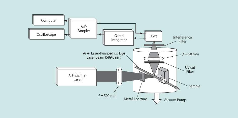
Fig. 1 Experimental setup for LAAF spectroscopy for surface analysis.
3. Results and Discussion
3.1 Removal performance of laser ablation
Figure 2 shows the depth profiles of ablation spots produced by 500 shots of nanometer-scale laser ablation in the previous study (a)7) and in this study (b). The spot areas were 4.4 and 1.3mm2, and the averaged ablation fluences were 26 and 38 mJ/cm2 for Figs. 2(a) and 2(b), respectively. As shown in Fig. 2(b), depth uniformity was markedly improved. The coefficients of variation of 21 and 6% were estimated from the bottom parts of Figs. 2(a) and 2(b), respectively. The y-direction profile in the case of Fig. 2(b) showed a similar quality to the x-direction one. This improvement seems to be due to the following: the discharge quality in the chamber of COMPex205 excimer laser being improved, very small area being extracted from the best uniformity area of the original beam and the ablation spot area being shrunk to 1/3 the previous one. In addition, loose focusing can weaken the effect of slant incidence on uniformity, hence the incidence angle tuning described above also gives good results on the improvement. Next, the removal rate of laser ablation was investigated under these new conditions. Figure 3 shows the plots of the ablation rate of the PMMA sample. Since ablation depth was proportional to the sample. Since ablation depth was proportional to the number of laser shots and LAAF signals from each shot were almost constant, ablation depth by each shot can be estimated to be constant. Laser ablation has a threshold fluence, and a fluence of more than 18 mJ/cm2 was needed to obtain constant LAAF signals in this case. The minimum ablation rate, which corresponds to the slope of each plot, was only 0.86 nm/shot when the ablation fluence was 20.9 mJ/cm2.
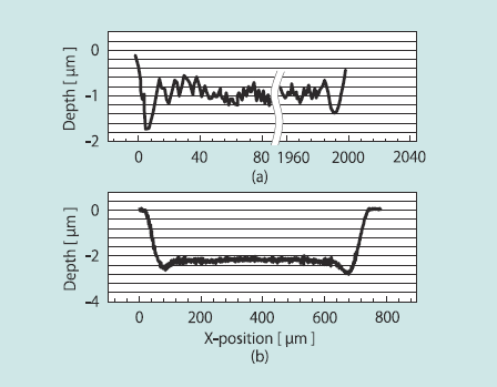
Fig. 2. Depth profile of ablated spot on surface of target sample ablated with 500 laser shots. (a) is cited from the previous work, and (b) from current work. Since the (a) profile was too wide, the middle part was removed.
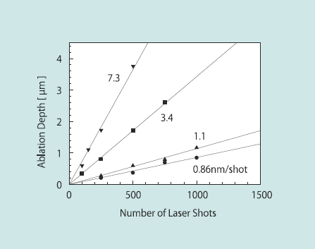
Fig. 3 Total ablation depth of target sample as a function of number of laser shots. The ablation fluences were 20.9 mJ/cm2 (circle), 22.8 (triangle), 33.1 (square), and 44.8 (reversed triangle).
3.2 Detection sensitivity
In the previous setup,7) the ablation spot area was approximately 2 x 2mm2. Thus, the optimized conditions were a probe laser beam diameter of 5mm and distances between the probe laser beam and the sample surface of 10 – 13 mm. A distance shorter than 10mm decreased S/N ratio with 5mm_ due to laser scattering light from the sample surface. In this work, since the ablation spot size was as small as 0.5 –1.4mm2, a smaller beam diameter and a shorter distance seemed effective. Through preliminary optimization experiments, a beam diameter of 1.5mm and a distance of 5mm were adopted. The pressure of buffer gas in the chamber of 1 Torr was used. Although the ablated volume was 1/3 –1/9 the previous work, the new conditions showed better S/N ratio than the previous ones.
LAAF and background signals were compared experimentally under the above conditions. Figure 4 shows LAAF signal intensities integrated temporally from the Na:PMMA sample, where only the ablation laser was injected in shots 0 – 50, the probe laser detuned from the Na D2 line was also injected in shots 50 –100, and the probe laser was tuned to the Na D2 line in shots 100 –150. The concentration of the doped sodium was 12.8 mg/cm3 and the ablation spot size was 1:6 x 0:86mm2. An ablation rate of 5.5 nm/shot was estimated. As shown in Fig. 4, no stray light of the laser beam from the target surface, ablated atoms and buffer gas was observed. Thus, there is still room for improvement in S/N ratio. The average of the LAAF signal part was 0.92 and the standard deviation of the noise part was 0.08. Thus, the signal-to-noise ratio of 11.5 could be estimated, and the absolute weight of sodium of 97 fg was calculated from the ablated sample with one shot ablation. Therefore the LOD of 25.2 fg, greater than the former result,7) could be estimated for the S/N ratio of 3. Hence, the system improvement resulted in the advancement in the LOD as well as in the depth resolution.
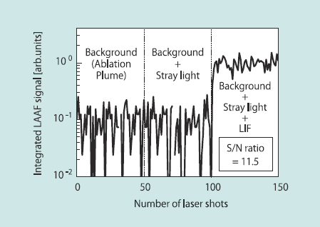
Fig. 4. LAAF signal intensities integrated temporally by each ablation shot. The intensities in shots 0 –50 are from laser ablation only, those in shots 50–100 are from laser ablation and the probe laser detuned from the Na D2 line, and those in shots 100–150 are from laser ablation and the probe laser tuned to the Na D2 line.
3.3 Experimental demonstration of nanometer-scale surface analysis
To confirm the experimental surface analysis with nanometer- scale resolution, a two-layered sample that has PMMA and Na:PMMA concentration of 4:2 x 10⁻⁴ g/cm3 was prepared by spin coating. Depth resolution was assumed as the number of shots required to distinguish the boundary of the layers. Figure 5 shows plots of the integrated LIF signal (x-axis) as a function of the shot number and depth (y-axis), that obtained around the boundary of the layers (PMMA/Na:PMMA) of the sample, where upper-side signals were from the blank (PMMA) layer and lower-side signals were from the Na:PMMA layer, the ablation fluence was 24 mJ/cm2 and the measured ablated rate was 1.2 nm/ shot. At the boundary, only three shots were taken to rise up from 10 to 90% of the mean of the Na:PMMA layer signal. This means that the signal of the blank layer could be switched to that of the Na:PMMA layer if the Na:PMMA laye’s thickness was larger than 3 x 1:2 nm. Therefore, the depth resolution of 3.6 nm was estimated from the result, and we can say that this is the first demonstration of a nanometer-scale depth analysis of a solid surface using LAAF spectroscopy.
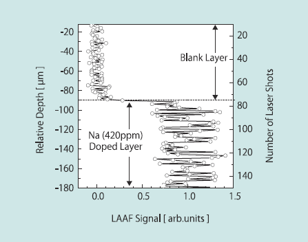
Fig. 5. Demonstration of surface analysis of nanometer-scale depthresolution.
3.4 Atomization efficiency
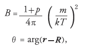
Though the nanometer-scale analysis was confirmed above, we also considered that the detection sensitivity has still room for improvement. To clarify the theoretical sensitivity performance of LAAF spectroscopy, atomization efficiency should be estimated. Thus, as a first theoretical analysis of LAAF, a numerical calculation program for the flight of an ablated sample was coded using the sputtering model described in Fig. 6.
The velocity distribution of sputtered particles by laser ablation is often represented by a Maxwellian distribution. The angular distribution is forward-peaked by collisions of the particles among themselves.8,9) Thus the density distribution n of
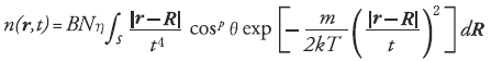
scattered particles from the ablation spot is given by where the S is the area of ablation, N is the number of target atoms in the ablated volume, θ is the elevation angle, t is time from the ablation, k is the Boltzmann coefficient, T is the temperature in the Maxwellian distribution, B is the normalizing coefficient, η is the atomization efficiency and p is the parameter that determines the angular spread of the plume.
We defined atomization efficiency as the ratio of the number of dissociated atoms to the number of atoms in the ablated sample at the position in which the probe laser beam was injected. The atomization efficiency η could be estimated by comparing the absolute intensity of time of flight profile of the experiment with that of the theoretical calculation. The LIF was calibrated with a thermal controlled Na cell for absolute sensitivity. As no deceleration of the particles was assumed in the calculation, the results were compared with those from LAAF experiments under vacuum. By varying p, T, and S, the experimental sodium density distribution was compared with the calculation results. Actually, neutral atoms are generated in the dissociation of the target and a recombination of ions and electrons in the atomization, and decrease in the recombination of atoms and other species. Thus, each efficiency must be considered. However, a recombination emission of the plume plasma was so weak that affect by the recombination of ions could be neglected. In addition, the recombination of the atoms was also negligible from the agreement between the experimental results and the calculation without consideration of such recombination. Thus, the atomization efficiency was regarded as equal to the dissociation efficiency in this section.
Figure 7 shows estimated atomization efficiency as a function of ablation fluence. T = 3000-13000 and p = 10-20 were used for fitting to the experimental results in this case. From the figure, it was found that atomization efficiency is affected by ablation fluence. An atomization efficiency of 5% was obtained approximately for the ablation fluence of 20.9 mJ/cm2. Consequently, an atomization efficiency range of 5–10% was obtained in nanometer-scale ablation. The improvement in atomization efficiency seemed difficult in the case of just above ablation threshold. Even if the atomization efficiency was improved, the improvement in absolute signal intensity would be limited to 10 – 30-fold. On the other hand, numerical simulation says that the absolute atomic density of the ablated sample is as high as 106–107 cm-3. Thus, the improvement in sensitivity can be expected by increasing LIF sensitivity and reducing background noise. So, LIF sensitivity improvement and theoretical investigations will be attempted in the future.
Fig. 6. Simplified atomic distribution model of LAAF spectroscopy.
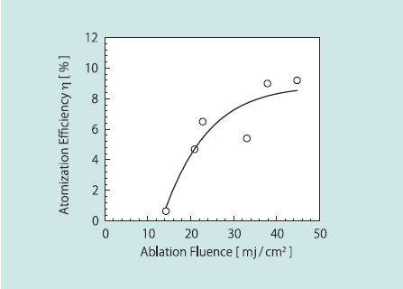
Fig. 7. Estimated atomization efficiency as a function of ablation fluence.
4. Conclusions
We improved the depth analysis system using LAAF spectroscopy for solid surfaces. An extremely high depth resolution of 3.6 nm was demonstrated using sodium-doped PMMA for the first time. An extremely high sensitivity of 25.2 fg was also obtained. Therefore, the LAAF spectroscopy could be applied to practical analyses such as that of the impurity distribution of a solid surface. Furthermore, an atomization efficiency of 5–10% was estimated by numerical simulatio
光と有機材料を利用した「ユビキタスセンシング技術」の開発
主な研究発表 OPTICAL REVIEW Vol. 12, No. 4 (2005) 301–306
Spectroscopic Applications
of Integrated Tunable Solid-State
Dye Laser
Yuji OKI, Shotaro MIYAWAKI, Mitsuo MAEDA and Masamitsu TANAKA1
Graduate School of ISEE, Kyushu University,
6-10-1 Hakozaki, Higashi-ku, Fukuoka 812-8581, Japan
1Seiko Electric Co., Ltd., 20-1, Tenjin 3-chome, Koga, Fukuoka 811-3197, Japan
(Received November 15, 2004; Accepted April 20, 2005)
A novel type of tunable laser is developed that integrates dye-doped plastics laser waveguides with a distributed feedback structure. The waveguide matrix is dye doped poly-hydroxyethylmethacrylate:methylmethacrylate, and a single-mode waveguide is achieved by refractive index control. The wavelength coverage is over 560–1100 nm using a frequency doubled Nd:YAG microchip laser. The miniaturizing of the optical-pumped solid-state dye laser extended the lifetime to more than million shots and decreased the required laser threshold energy to less than 1 µJ. Novel type spectroscopic applications using the multiple wavelength laser array chip are also proposed and demonstrated. © 2005 The Optical Society of Japan
Key words: dye laser, plastic, PMMA, spectroscopy, distributed feedback, waveguide, NIR spectroscopy
1. Introduction
Tunable lasers are the most important tools for spectroscopy. Recently many solid-state tunable devices, such as Ti:sapphire lasers and optical parametric oscillators, have been developed and their performance has been improved considerably as compared to the traditionally employed liquid dye lasers. However, the whole system is still complicated, bulky and expensive, and maintenance-free operation is difficult. These problems restrict laser spectroscopy from spreading to various industrial applications.
As an alternative, we are studying integrated tunable lasers, where a laser material, a tuning element, an optical cavity and a pumping source can be integrated on a planar waveguide. With this approach, a better stability is expected, since the integration makes a tunable laser device robust. Though it is not easy to realize totally integrated tunable lasers at present, a reasonably compact laser should be possible by using several techniques such as an optical waveguide, an optically-pumped laser, and a distributed feedback (DFB) technique.
A distributed feedback (DFB) technique that is often employed in semiconductor lasers was introduced on an optical waveguide made of an organic material in this work. Integration of the DFB structure allowed a mirror-less laser cavity on a plastic film that can be fabricated easily by a spin-coating and a subsequent photo-fabrication technique. Previously the DFB laser action was obtained by the interference of two pumping beams in the active medium.1–3) We have also reported on ‘holographically’ pumped DFB lasers with dynamic grating formed on dye-doped plastic waveguides.4) Narrow-band tunable laser action around different wavelengths in the visible region was obtained by pumping with a frequency doubled or tripled Nd:YAG laser. Most solid-state plastic dye lasers have a limited durability problem, some approaches were made in an attempt to improve the durability.5–7) Our approach to the waveguided DFB laser action demonstrated very low laser threshold, narrow spectral width and relatively long durability.
In this paper, an integrated laser system based on an allplastic DFB dye laser waveguide is reported. A multiwavelength laser waveguide array is introduced, and evaluations of the waveguides developed are described.8,9) This study covered development of channel type waveguide DFB lasers that have a permanent periodical structure and are termed ‘DFB lasers’ in contrast to the holographically pumped DFB laser, and evaluation of their laser performance. Finally, spectroscopic applications based on multiwavelength DFB laser array chip are demonstrated.10)
2. Experiments
Figure 1 shows the fabrication process for the DFB laser array chip. A dye-doped film was first spin coated on a poly(methyl methacrylate) (PMMA) substrate using the prepolymer method.11) Depressure-distilled MMA monomer was mixed with laser dyes using a delivery such as an ethanol or a propylene carbonate (PC), then the mixture was radically polymerized by heating at a temperature of 60 – 75°C. An initiator of 2-2' azo-bis-isobutyl-nitoryl was used to start the polymerization.
To attain a single mode propagation waveguide, the refractive index modification was used in some cases and the p(MMA:HEMA) copolymer was used in others. Before the complete polymerization, the MMA pre-polymer was spincoated on the PMMA substrate and an active layer was formed. After spin-coating, the polymerization was completed by post heating at 75° for 6 h, and a planar laser waveguide was fabricated. The concentration of a laser dye can be calculated from the measured absorption coefficient and the thickness of waveguides, and it must be as high as 10 – 30mM to obtain a laser operation with transverse pumping. The laser performance of the active medium was investigated in this step by producing a holographically pumped DFB structure and observing the laser operation.
In the next step, a multiple stripped-waveguide structure was fabricated using the ultraviolet (UV) lithography technique. A KrCl* excimer lamp (USHIO, UER20-222, 7mW/cm2) was used for the exposure and a mixture of ethylicetate (1) and isoimylicetate (9) was used as an etchant. Then the output sides of the was used as an etchant. Then the output sides of the waveguides were polished. Typically, 10 µm wide and 20mm long waveguides were used in the experiments. Finally, the DFB structure was written by exposing with interfering UV beams. Figure 2 shows the experimental setup for the exposure. The frequency quadrupled (FHG, 266 nm) and a Q-switched pulsed Nd:YAG laser (Continuum, SureliteIII- 10 SHG) was used. The SHG and FHG beams were separated from the fundamental laser beam with dichroic mirrors, superposed again, and then the beams were injected onto the waveguide at the same incidence angle. The injected beams were sheet-formed (0.5 x 20mm2) with two cylindrical lenses. An Al-coated mirror was attached on the waveguide film at a right angle to obtain an interference of the beams. The incidence angle θ could be changed by just rotating the waveguide. The wavelength accuracy of 0.1 nm was corresponded to the angular accuracy of 0.001° of the rotation. The accuracy of 0.02 was also required on the effective refractive indices at lasing wavelength. Therefore, the monitoring using the SHG injection was very effective in determining the incidence angle.
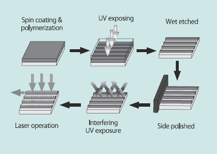
Fig. 1. Fabrication process of DFB dye laser.
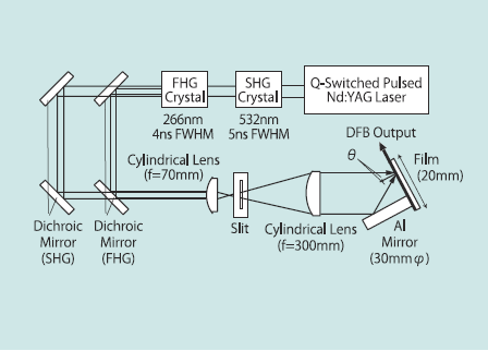
Fig. 2. Experimental setup for interfering UV exposure.
3. Laser Performance
The DFB dye laser waveguides can be pumped with a very simple optical system as shown in Fig. 3. A frequencydoubled, LD-pumped micro-chip-Nd:YAG (λ = 532 nm, Nanolaser Corp., PNG-002025-040) was used as a pumping source. The output pulse energy was 40 µJ and the pulse duration was 0.5 ns. The pumping beam was expanded horizontally by a Powell lens (spread angle of 45° at 532 nm), focused vertically by a cylindrical lens ( ƒ = 40 mm), and injected transversely on the DFB plastic dye laser waveguide. The pumping laser beam size was fitted to the waveguide area. Though the laser output was obtained from both ends of the waveguide, only one end was used in the following experiments. Selection of each strip could be made without any re-alignment just by scanning the substrate vertically. As mentioned in the previous section, eleven kinds of laser dyes were evaluated with holographically pumping. For the prefabricated DFB laser, the spectral coverage of fourteen different kinds of dyes or dye-mixtures was evaluated, and the results are shown in Fig. 4.
Since the output wavelength from each DFB waveguide was fixed, each plotted mark corresponds to the output from each of these waveguides. Generally, the covered spectral region of the DFB lasers wider than that of the holographically pumped DFB laser due to the difference of the order m of the Bragg reflection and the coupling coefficient of the DFB structure. For instance, the spectral coverage range of LDS722 DFB laser was about 60 nm in this work as compared to 40 nm with the holographic DFB. The whole demonstrated tunable region covered from 560 to 1100 nm.
Subsequently, spectral narrowing properties were also evaluated for several kinds of dyes using a spectrometer (resolution of 0.1 nm) and a solid etalon (free spectral range = 1 cm-1@ 500 nm). As a typical case, a fringe pattern of the laser doped with rhodamine640 from the etalon is shown in Fig. 5. The spectral width of 36 pm was calculated from the pattern, and the spectral widths of 30 and 27 pm were also obtained from DCM and LDS722, respectively.
Based on the coupled wave theory12) related to the output spectrum, the stop band of the DFB structure was estimated to be 15 pm by considering the measured coupling coefficient of 1.74 cm-1 for usual DFB dye laser. The split spectrum, such as shown by a semiconductor laser with a uniform DFB structure, could not be resolved because it was too narrow. Recently, the split spectrum was observed experimentally from some DFB dye lasers fabricated by extensive UV exposure, and employing a high-resolution monochromator (40 pm resolution). The intensity of the two peaks was not balanced, instead only one peak was outstanding. The widest stop band was about 160 pm. No split spectrum could be resolved from the usual DFB lasers. Generally, the wavelength stability of less than the bandwidth is needed for spectroscopic applications. However, the output wavelength can alter slightly due to change in the temperature and change in the refractive index caused by the dye degradation. We expect that a temperature control will solve this problem in future.
Figure 6 shows examples of the output characteristics of the DFB dye lasers, where the dopant was rhodamine590 with a concentration of 15.9 mM. The waveguide length and width were 14mm and 100 µm, respectively, the thickness was 4.5 µm, the pumping repetition rate was 100 Hz, and lasing wavelength was 585 nm. Based on the output characteristics, the laser threshold energy and slope efficiency were measured as 0.52 µJ (37 µJ/cm2) and 0.98%, respectively. The threshold energy was only 10% of the threshold of 6 µJ in the case of 6ns pulse pumping (flashlamp-pumped Nd:YAG laser; Surelite III), and less than 1% of that for the holographically pumped DFB (57 µJ) laser. Several reasons can be considered for the low threshold: 1) the waveguide structure confines the excited laser-dye molecules so structure confines the excited laser-dye molecules so that, higher exciton density can be obtained than in the bulky dye laser, 2) the DFB laser uses the high efficiency of fundamental order Bragg reflection, and 3) the pulse duration of a pumping beam was as short as 1 ns decreases the pumping energy required and reduces the heating effect.
Durability of the DFB waveguides was also evaluated as shown in Fig. 7. The lifetime was measured in terms of number of shots corresponding to decrease in the output energy to half of its initial value. The lifetimes of 2.9, 5.5 and 6.3 million shots were obtained with different waveguides doped with rhodamine590, rhodamine640 and LDS798, and with the pumping energies of 1.3, 3 and 1.8 µJ, respectively. DCM laser dyes also show a lifetime over one million shots. In the case of LDS798, the output energy was increased during the shot count of less than one million shots. Since the pumping repetition rate was 100 Hz, 5 million shots correspond to a life of about 14 h, which should be sufficient for a spectroscopic experiment. The lifetime of 0.06 million shots was obtained in a holographically pumped DFB laser of thodamine590 with flashlamp-pumped Nd:YAG laser,11) and the lifetime of this work is approximately 100 times that. The reasons for a long lifetime are believed to be as follows: 1) very low pumping energy could have suppressed the dye degradation, 2) the heat caused by the optical pumping in the waveguide could be dissipated rapidly, 3) 5 –10 times higher doping concentration can also extend the life of a DFB laser. Further, the lifetime can be practically extended many times by fabricating multiple-waveguides on the same substrate and rapidly exchanging the waveguide without any separate optical alignment.
One useful application of this laser is in absorption spectroscopy. For such application, a high repetition rate and stable laser operation are important. Figure 8 shows the DFB output energy as a function of the repetition rate for different dye doped waveguides. No cooling system was needed with a high repetition rate of 1000 Hz. In the case of rhodamine640, LDS950, Stylyl20, LDS950 + rhodamine640 and Styryl20 + rhodamine590, the output energies were decreased by 20 –30% when the repetition rate exceeded 500 Hz, and this seemed to be due to the triplet-state absorption. On the other hand, DCM and LDS722 showed no significant change in the output, even when the repetition rate was increased to 1000 Hz. The pulse-to-pulse stability of the DFB output energy was also evaluated at a repetition rate of 100 Hz. The standard deviation of the fluctuations for 1000 pulses was measured as only ±0.64% (rhodamine590). Since the measured fluctuations of the pumping laser were ±0.57%, the stability was expected to be less than ±0.5% and the DFB dye laser output was confirmed as a very stable light source. Stable operations were also observed with the dyes DCM and rhodamine640.
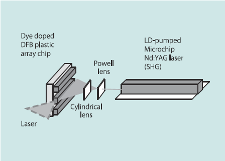
Fig. 3. Schematic of experimental setup for DFB plastic dye laser pumping.
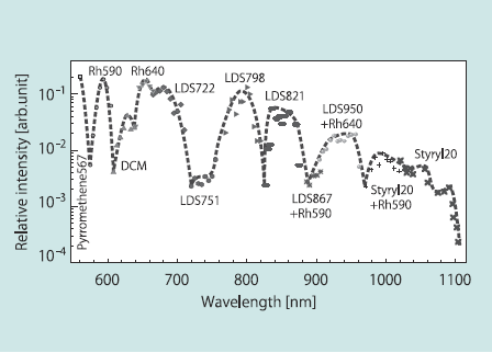
Fig. 4. Spectral coverage of the DFB plastics dye laser with twelve different kinds of laser dyes. (Fourteen dyes or dye mixtures were evaluated, and twelve of them were sufficient for covering this range.)
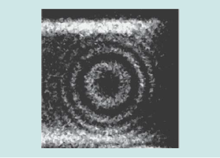
Fig. 5. Fringe pattern of DFB laser output by Fabry–Perot etalon (Dye:Rhodamine640, FSR=1 cm-1).
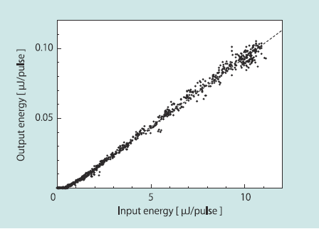
Fig. 6. Output pulse energy of Rhodamine590 doped DFB laser as a function of input pumping energy.
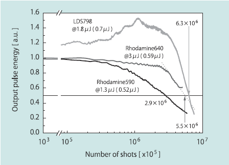
Fig. 7. Durability test for waveguides doped with rhodamine590, rhodamine640 and LDS798. The lifetime was decided based on number of shots corresponding to decrease in the output to half of the initial value.
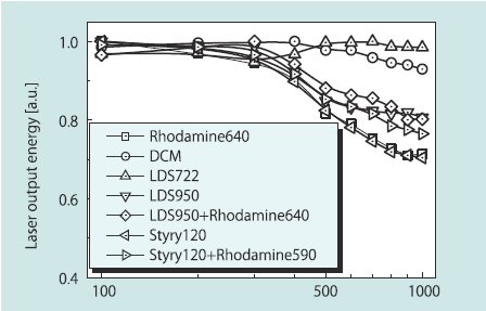
Fig. 8. DFB laser output intensity as a function of repetition rate of pumping.
4. Spectroscopic Applications
4.1 Multi-wavelength dye laser array
One of the advantages of our laser is that several tunable waveguided DFB lasers with different output wavelengths can be integrated on a plastic chip. Based on the multiwavelength laser array chip, a spectroscopic application with a novel concept is proposed in which multi-wavelength output within a scanning range can be used; the scheme is termed “digital spectroscopy". The traditional scheme with wavelength scanning, in contrast, is termed “analog spectroscopy".
Figure 9 shows the spatial intensity distribution at the surface of the photodiode array (a), and the digital absorption spectrum (b) obtained from the “digital spectroscopy" experiment.10) Figure 9(a) shows measured intensity of the laser beams from the DFB laser array that has nine waveguides with Bragg wavelengths ranging from 589.8 to 590.7 nm with 0.11 nm pitch. The solid line represents the intensity of the multi-laser output after passing through a sodium vapor cell, and the dashed line represents the reference intensity. Since each peak position in (a) corresponds to the wavelength of each waveguide, the reconstructed profile (b) clearly shows the absorption spectrum digitally that represents sodium D1 and D2 lines. This scheme has an advantage in that the spectral resolution is determined by the previously designed wavelength/combination of the laser array, and not determined by the spatial resolution as in a monochromator. Therefore, very high spectral resolution can be expected with a large observation area in comparison with the use of a monochromator in a traditional approach. Further, random-pitch-scanned or wide-scanned spectra can be obtained by this scheme without spectral scanning.
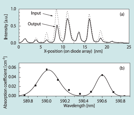
Fig. 9. The sodium absorption measurement using ‘‘digital spectroscopy’’ scheme. (a) spatial intensity profile of output from nine laser waveguides on a chip through the sodium vapor cell, (b) reconstructed absorption profile from (a).
4.2 Near infrared spectroscopy
Another application involved a laser chip recorded at three splitter wavelengths. This technique was applied to polymerization monitoring in a plastic synthesizing process. PMMA was selected as a target sample in this demonstration. Since MMA monomer changes its near-infrared (NIR) absorption spectra when it is polymerizing, a remote monitoring technique combined with imaging can be considered.
At first, a wavelength for the image monitoring with a Silicon-CCD camera was selected. MMA was polymerized in a method similar to that described for the integrated lasers, and NIR absorption spectra of the partially polymerized MMA were measured. Figure 10 shows enlarged differences of spectra between the just started and the partially polymerized state. A ridge rose up at around 890 nm with increasing polymerizing time, which can be related to the third harmonic of an asymmetrical elastic vibration of methylene radical. The ridge seems to represent the modulation of methylene radicals in MMA due to the polymerization, and is defined by the following equation:
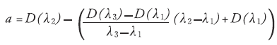
to calculate polymerization-indices a based on the preliminary experiment. The wavelengths λi(i=1,2,3) were monitoring wavelengths and their values were 872.5, 890.5 and 911.5 nm, respectively. Based on preliminary experiments, it was found that the index a can represent the polymerization progress.
Figure 11 shows the experimental setup for the monitoring with a DFB laser chip that could operate at λ(1,2,3). The laser array was pumped with a LD-pumped microchip Cr:Nd:YAG at a repetition rate of 100 –1000 Hz, and the laser output was injected into a sample cell. The transmitted laser output was measured with a CCD camera, and recorded as a 2D-image. Subsequently, the intensity image of a was calculated and analyzed. Figure 12 shows a typical example of experimental results. Since the sample was stirred during the polymerization, the a intensity as almost uniform in the cell, and the image intensity became brighter with increase in the polymerizing time as shown in Fig. 12. Based on these results, the integrated laser is useful for such an application that requires several specified wavelengths.
Fig. 10. Difference in optical densities of polymerizing MMA and pure MMA at wavelength region around 900 nm by varying polymerization times.
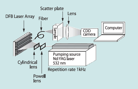
Fig. 11. Experimental setup for the polymerization state spectroscopy with DFB laser array.
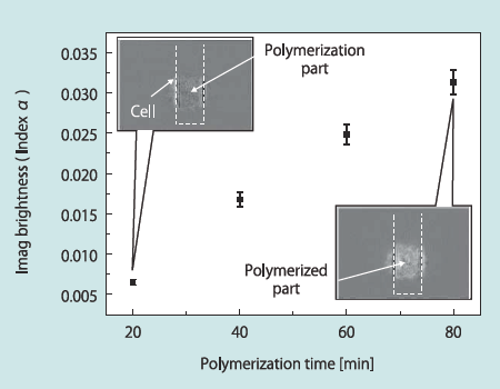
Fig. 12. Infrared images and absorbance of polymerizing PMMA as a function of polymerizing duration.
5. Conclusions
Integrated tunable laser array systems on a plastic chip have been presented. The distributed feedback dye laser waveguides were fabricated by a spin coating, UV lithography, and interfering UV exposure techniques. Laser threshold energy of less than 1 µJ, and a durability of more than six million shots were attained. A spectrally narrowed (width = 0.04 nm) tunable output ranging from 560 to 1100 nm was also demonstrated. Finally, with a tunable laser-array, novel schemes for spectroscopic applications were proposed and demonstrated.
Acknowledgement
This study was carried out under the Photonics Project program sponsored by Fukuoka Industry, Science and Technology Foundation (http://www. ist.or.jp).
光と有機材料を利用した「ユビキタスセンシング技術」の開発
CAMPUS LAB 26 大学研究室を訪ねて
主な研究発表 レーザー研究(2012.12)
微小流体光学に向けた
チップ内組み込みレーザーの研究
Development of Integratable Laser for Optofl uidic Chip
鍬光 浩太1,吉岡 宏晃1,片岡 周作1,†,鳴石 奈穂子2,田中 喜秀2,興 雄司1
1九州大学大学院 システム情報科学研究院( 〒819-0395 福岡市西区元岡744)
2産業技術総合研究所 健康工学研究部門( 〒563-8577 大阪府池田市緑丘1-8-31)
Kota KUWAMITSU,1 Hiroaki YOSHIOKA, Shusaku KATAOKA,1
Nahoko NARUISHI,2 Yoshihide TANAKA,2 and Yuji OKI1
1Faculty of Information Science and Electrical Engineering, Kyushu University,
744 Motooka, Nishi-ku, Fukuoka 819-0395
2Advanced Institute Science and Technology (AIST),
1-8-31 Midorigaoka, Ikeda, Osaka 563-8577
Received August 19, 2012
Integratable and disposable solid-state dye lasers with a distributed feedback waveguide structure were studied. We fabricated the coupling of a methacrylate copolymer waveguide and similar substrate and demonstrated primitive fl uorescence detection. We also developed laser integration on a beam-shaper with an optical fi ber for fl uidic chips of polydimethylsiloxane.
Key Words: Optofuidic, Microfl owcytometry, Dye laser, Waveguide, PDMS
1. はじめに
有機色素レーザーはレーザーの初期より研究されてきたレーザーである。有機蛍光分子は,分子設計により様々な波長特性の設計が可能で、高いスペクトル輝度と誘導放出断面積を持つ一方、短い蛍光寿命に起因する高い励起光強度と光化学反応などによる分子構造の変性による劣化が不可避である。媒質が液体であれば、循環系や成型の為のセルなどが必要で総じて複雑であるものの、劣化問題はさほど問題にならないが、有機溶媒の可燃性やコンタミネーションの問題から一般での応用は難しい。そこで、固体レーザーが主要なレーザー装置となる一方で、可燃性・汚染問題解決のアプローチの一つとして、有機分子を固体レーザーとして発振させる研究もこれまで行われてきた1‒4)。 我々は、固体色素レーザーの利点として液相プロセスが可能な高分子マトリクスに着目し、有機導波路構造を印刷的技術で構築するプリンタブル導波型レーザーの研究を行ってきた5)。特に微小アプリケーションのチップ内に直接レーザーを構築することで、励起光としての固定波長レーザー光をアプリケーションに必要な波長に変換して必要に応じて近接照射できる。将来的に有機LDの発振はこうしたデバイスをさらに発展させることが予測できるが、光励起レーザーであっても現実的な出力強度で、調整・メンテナンス不要な使い捨て光源が可能となる点で興味深い。本稿では、optofl uidicチップの一例としてマイクロフローサイトメトリーチップを対象の一つに、有機固体レーザーを組み込む上でのポイントを研究した結果について報告する。
2. レーザー作製プロセスとアラインメント
Fig. 1にプリンタブルプロセスを示す。これまで高分解能ディスペンサー( 武蔵エンジニアリング、ML-5000XII)と細線描画用SUSニードル(岩下エンジニアリング、PRN0.06、内径0.06mm)を組み合わせたロボット描画装置を利用して、断面幅 60µm〜120µmの導波路直接描画を行ってきた、我々が開発した無溶媒プレポリマーペン描画法(以降ペン描画と呼称)では、高粘度状態のポリメタクリル酸メチル(PMMA)と未重合のメタクリル酸メチル(MMA)の混合状態の「プレポリマー」を作製し、これに色素を混合してペン描画に利用する。描画後のポストアニール(72℃、120 min)によりMMAを蒸発あるいは重合させて固化を完了し、その後回折格子を記録することで分布帰還構造(DFB)を作製する6)。導波路は縦シングル横マルチモードにすることで出力を増やす構成になっており、膜厚は3〜5 µmとなるが、膜厚が一定でないとDFBの発振スペクトル幅が拡がったりASEなどによる広帯域な成分が増大したりする。
微小ストライプの描画後固化において、低粘度溶液はマランゴニ対流が支配的になり、断面プロファイルがM字型に、高粘度溶液では∩字型となる。しかし、ペン描画法では、導波路の屈折率制御にも利用するメタクリル酸2-ヒドロキシエチル(HEMA)との共重合プレポリマーのブレンド比率を調整することで、両者の中間点の台形型の断面プロファイルを得ることが可能である。この場合、導波路の中央部分には厚さの変化がないフラットトップとなり、良好なレーザースペクトルを得ることができる。
マイクロフローサイトメトリーにおける流路の断面寸法は60〜100µm程度が一般的で、ここにレーザーを近接照射する際にはビーム幅はこれらよりも細い30µm以内に抑えるのが理想的である。Fig. 3に、レーザー導波路を組み込んで直接励起光を流路内に結合させる時、考え得るアラインメントを図示する。流路を維持するためにポリマー素材では隔壁の厚さが数10µm以上必要であり、そのため、レーザー出射部から50µm程度伝搬したビームが流路と鎖交した時のビーム幅が分解能を決定することになる。よって、レーザー導波路の組み込み向きはシングルモードの閉じ込め方向を流路の流れに平行に配置する(a)と、垂直に配置する(b)で異なる。
配置(a)ではシングルモード閉じ込め方向のビーム広がりが大きくなる。屈折率構造が対称であるシングルモード導波路の基本TE0モードであれば、ガウスビーム理論計算でビーム広がりを近似でき、ビーム出射位置のフィールド幅を5〜7µmにしないと条件を満足できない事が予測できる。しかし、波長600 nmでコアを5µmとするとシングルモード条件を満足できない。また、レーザーを横励起する場合、励起光をシート状に成形・入射する方向は流路に沿った方向となり、励起光光学系をチップに埋め込まないと励起がしにくい。
配置(b)は作製が容易である一方、マルチモード閉じ込めの方向が流路内での分解能を決めるため、導波路の幅を20〜30µm程度まで狭める事が望ましい。しかし、PRN0.06ノズル内径は0.06 mmであり、描画幅60〜100µmでは分解能も上がらない。
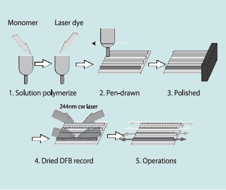
Fig. 1. Process for printable waveguide of DFB laser array.
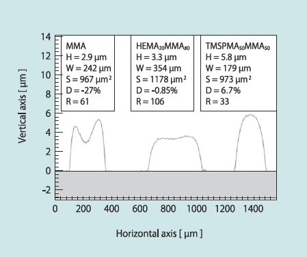
Fig. 2. Measured waveguide cross section profiles in various copolymer composition.
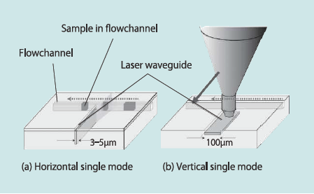
Fig. 3. Laser alignment for microflowchannel coupling. single mode confi nement direction is parallel (left) and perpendicular (right) to the fl ow direction.
3. PMMAを利用したプロトタイプチップ
3.1 作製手順
まずはPMMAのプロセスのみを利用した単純な流路チップへの組み込みを行った。作製の容易な配置(b)をここでは採用した。既にエキシマーレーザーのマスク露光によるレジストを用いないプロセスを用い、チップの作製とレーザーの組み込みを行ったプロセスをFig. 4に示す7)。 KrFエキシマーレーザー(Lambda Physik、COMPeX 110)で石英マスクを通してPMMA基板を露光し、ウエットエッチングで深50µmのレーザー用溝と、深さ90µmの流路溝を作製する。その後、ペン描画により、クラッド層を描画し、その上にレーザー層を作製した。レーザー層は色素の添加により屈折率が0.004程上昇することを利用して導波路を構成している。レーザーは右下のように流路の高さから見て中央に配置されている。描画で作製したチップでは導波路端でレーザーが乱されるため、この部分には屈折率をそろえたp(HEMA:MMA)を埋めることでビーム散乱を抑えた。DFBを作製後、電極をリザーバーに取り付け、電解質とゲルを流路に詰めた。
Fig. 5は作製したチップの外観である。流路設計は屈曲させてチャンネル長を95mmまで伸ばし、流路の最後の部分には色素として、rhodamine590、pyrromethene567、LDS722、LDS798の4種類の色素をドープしたレーザーを組み込んだ。それぞれの発振波長は590、600、580、690、790nmである。4つの15 µLのリザーバーには白金電極をセットし、R1にNileblue690等の色素を注入後、リザーバーR1-R2間に40V/cmの電圧をかけて十字点まで導入後、R3-R4に70 V/cmをかけてFig. 5下のように電気泳動で試料を切り出した。
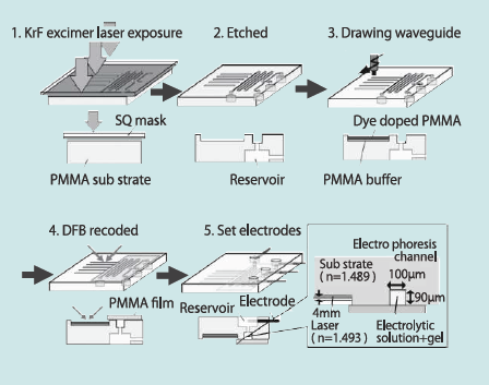
Fig. 4 Process of PMMA flowchannel and laser waveguide.
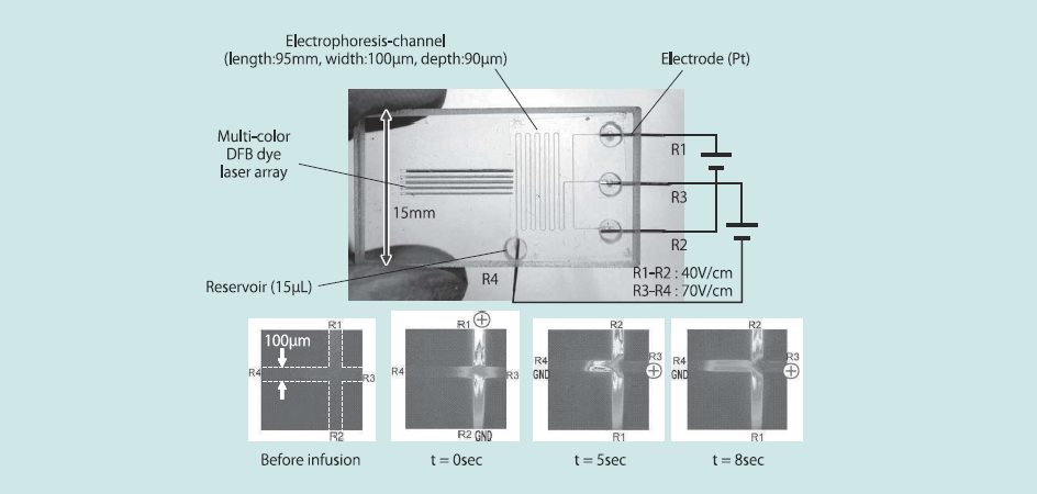
Fig. 5 Photo image of prototype of PMMA fl owcytometry chip with laser (above) and sample infusion at cross point (below).
3.2 レーザー特性評価と電気泳動実験
Fig. 6は一つのレーザーのスペクトルと、それによる蛍光のスペクトルである。レーザー光は600 nmに同調してあるが、励起光である532nmも観測されている。ノイズとなるのは蛍光の波長域700nm付近まで伸びているレーザー導波路からの色素蛍光(ASE)であるが、色素濃度の調整とDFB構造を強めに作製する事で、レーザーピーク強度の10-4程度まで抑える事に成功している。濃度を変えて計測した結果、背景光レベルが200nM相当であり、背景光の除去の工夫がまだ必要であるものの、初めて組み込みレーザーによるLIF(Laserinduced fluorescence)計測に成功した。
最後に、切り出し後にレーザー(600 nm)を励起しながら流路中を電気泳動する試料からの蛍光を検出した。Fig. 7にその結果を示す。泳動開始から4150秒後をピークとして、時間パルス幅が473乗となり、理論段数はN = 5.55(TP/WT)2により427であった。これは一般的なクロマトグラフィより劣るが、屈曲の多い流路を利用したのが理由であると考えられ、また、レーザーのアラインメントが(b)型でレーザー幅も100µmと広いことも原因の一つであると考えられる。こうした結果から、Fig. 3 (b)の構成ではなく構成(a)でのレーザーの組み込みを考え、同時に実際のマイクロフローサイトメトリーチップに近い設計での実験を行うため、作製組み込み対象をPDMS、配置(a)を採用して研究行う必要性が明らかになった。
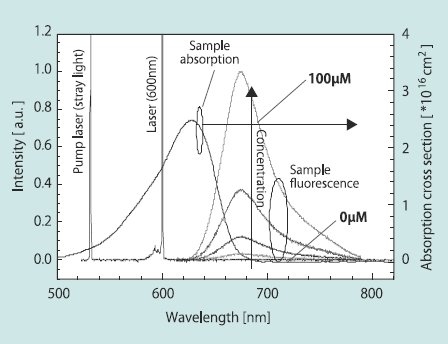
Fig. 6. Spectra of DFB dye laser, pumping laser stray light, and fluorescence from samples of which concentration is 0~0.1 mM.
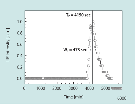
Fig. 7. Temporal modification of laser induced fluorescence from fabricated chip. Sample is nileblue690 and laser dye is rhodamine590.
4. 励起光学系集積レーザーのPDMS組込み
本節では、励起光学系の面内組み込みと配置(a)採用に伴う問題点の洗い出しを目的に研究を行った。前述の実験ではレンズを組み合わせた光学系で励起光をシート状に集光する光学系を利用し、チップ上方から入射していたが、配置(a)では光学系をPDMSチップの厚さ1〜2 mmの空間に埋め込む必要がある。ペン描画を最大限に利用した作製法で組み込みアラインメントを調査できる組み込みレーザーを作製した8)。
4.1 作製手順及び組み込み手順
Fig. 8に設計した組み込み型集積レーザーの概念図を示す。PMMAフィルム(125µm厚)を用い、光ファイバをこれに結合してビームを一方向にのみ広げるビーム成型フィルムを発案した。Shaperの端面を光学研磨し、この上にペン描画法により屈折率差を小さく設計した三層を積層描画した。なお、コア膜厚を安定させるため、クラッド層は125µm幅一杯に、コア層は60〜100µm幅に抑え、2層描画後にDFB構造を記録後、第3層をコートした。このように幅125µmのエッジ領域に同系ポリマーを3層積層することは従来のスピンコート等では不可能であり、ペン描画により初めて可能となったと言える。ポストアニール後、ウルトラミクロトーム(Sorvall社、UltraMicrotome MT-1)を用いてレーザーの出射面を作製した。各導波路の屈折率制御は共重合ポリマーp(MMA1-x:HEMAx)で主に行い、屈折率の校正はプリズムカプラー(メトリコン社、Model2010)により波長633 nmに対する実測値を元に行なった.
Fig. 9はPDMSチップへの組み込み手順を示す。PDMSチップを作製するモールドマスターとしてはSU-8 3035(マイクロケム)を用いてSiウエハー上に作製し、流路断面サイズは60 µm□とし、屈曲のないストレートのパターンを用いた。これに作製したレーザー付きビーム成型フィルムとクリーブした石英光ファイバ(125µm径、105µmコア)をそれぞれ独立でアラインメントした後、PDMSを接合部に投入してアラインメントを調整しつつ固定を行なった。レーザー出射光が流路位置にあるSU-8に照射するアラインメント調整を行い、レーザー出射部と流路の距離は60〜70µmに調整して固定した。固定後全域にPDMSを注入し、チップを完成させ、固化後にモールドマスターからリフトオフしてPDMS薄膜で蓋をしてチップとした。PDMSには室温硬化型高精細PDMS(信越石英,SIM-360)を用いた。
作製例の写真をFig. 10に示す。写真中央には rhodamine 6Gを利用したDFBレーザーが埋め込まれており、レーザーへの励起光入射は光ファイバからビーム成型フィルムを経由してチップ外への光の漏れが無いように行われている。組み込まれたレーザーの長さは5 mm、膜厚は3 µmでクラッドとの屈折率差は0.0015程度に設計した。Fig. 10の左下はレーザー出力部とマイクロ流路の結合部の顕微鏡写真であり、レーザーと流路の距離は70µmとし、レーザー出力が流路と鎖交する様にアラインメントを調整している。レーザー導波路の屈折率設計はコア1.495、クラッド1.493となるよう、共重合ポリマーのHEMA添加率をそれぞれ5%、2.5%とした。コア厚は約3.5µmである。周囲のPDMSは屈折率が1.408でこれもビーム成型フィルムではクラッドとして機能する。
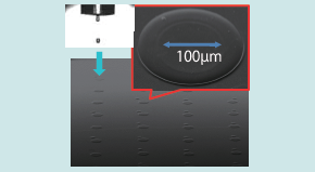
Fig. 11にクラッドによるビーム広がりの抑制の結果を示す。実測ではレーザーを無固化のPDMS中で動かし、流路との距離を変えながら流路側壁の散乱光を顕微鏡CCDカメラ(Nikon eclipse Ti)で観測し、画像処理後ガウシアンフィットしたビームプロファイルから半値幅を求め、ビーム広がり角を求めた。クラッドによる広がり抑制層がない場合、コア層厚3.5 µmに対して広がりは95 mradであった。対して、クラッディングを施したレーザーは10〜19 mradが観測された。Fig. 11に計算によるガウスビーム広がりを示すが、計測結果(○マーク)から出射時のビームフィールド全幅(e-2)は7µmと見積もられ、コア厚は3.5µmより大きくはみ出させることに成功している。対して、広がり防止がない場合、非対称導波路の為か広がりが大きく3.5µmフィールド幅の計算結果とも合致しない。一方でビーム絶対幅の観測結果(●マーク)は共に同様の理論計算(破線)より20µm近く大きな値が得られている。これは観測系の分解能の問題などが考えられるが、ビーム広がりを抑える事で流路に鎖交するビーム幅を、ほぼ30µm一定にできた.
コア・クラッドの屈折率差を0.001とする場合、コアにドープされた色素に起因する屈折率異常分散が屈折率差に与える影響を無視できない。色素添加による屈折率変化はこれまでも考慮して設計を行ってきたが、今回、色素をpyrromethene567に変更して発振波長を570 nmと短い領域に設定した際、シングルモード設計されていたにもかかわらず導波モードが2つ確認され、設計通りの結果を得ることができなかった。屈折率の異常分散を吸収バンドと誘導放出バンドをローレンツプロファイルでフィッティングして計算すると、pyrromethene色素分子の密度8mMで屈折率変化量の概算は発振波長域で0.001〜0.002程度と見積もられ、励起の反転分布の状況での変化も無視できない事が分かった。このため、屈折率設計には色素添加による正常分散屈折率の増減だけでなく異常分散や励起条件までも考慮する必要があり、実験による発振特性を確認しながら屈折率設計を行なう必要性も明らかとなった。
蛍光測定光源用レーザーとしてもう一つ重要な条件として、長波長側の背景光成分の低減がある。励起された蛍光色素の発光波長と同じ波長域のレーザー光成分は観測用フィルタでカットできないためDFBレーザーにおいてどの程度抑えるかが重要である。発振波長よりもおいてどの程度抑えるかが重要である。発振波長よりも10nm長波長側の線強度は通常の色素レーザーでは10-3程度の抑制率であるが、色素濃度を下げるあるいは色素の蛍光波長の長波長域での発振用いることにより,2 x 10-4程度まで低減することができている。
最後に、色素レーザーと流路間のアラインメントを行なうため、流路に流れる色素から蛍光を観測している様子をFig. 12に示す。右の流路は校正用の流路で、左は測定用である。標識色素Cy5®とスペクトル特性が類似している色素として、1,1,3,3,3',3' hexamethylindodicarbocyanineiodide(HIDCI)水溶液を使用して測定を行った。校正用流路での蛍光幅は38µm程度となっている。
このようにレーザー組み込みチップにおける問題点を一つ一つ解決し、蛍光検出実験を行なう段階まで現在研究は進んでいる。一方で、問題点も明らかになっており、良好な蛍光信号を得る事ができる歩留まりや作製手順の煩雑さから、次のステップとしてPDMSチップに直接描画する手法への回帰も検討中である。現在20µm細線描画に部分的に成功しているため構成(a)によるアラインメントでもPDMS内組み込みで分解能をある程度確保できる見通しがある。
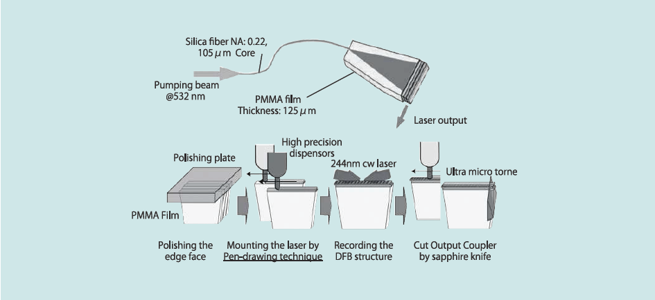
Fig. 8 Schematic of laser on organic-film beam shaper and its fabrication process.
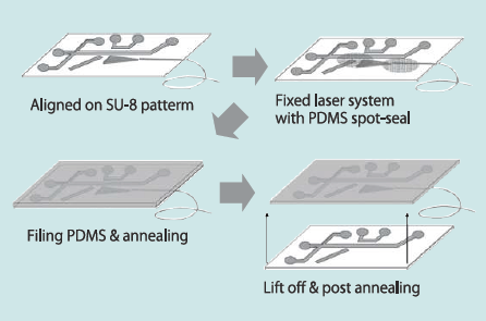
Fig. 9. Integration procedure of laser and organic film beam shaper into PDMS fl owcytometry chip.
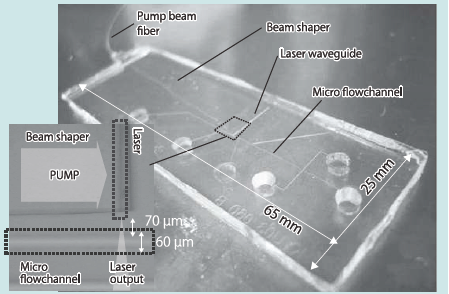
Fig. 10. Photoimage of PDMS chip with integrated laser waveguide and organic film beam shaper. Inset (left below) is the microscopic image of coupling point.
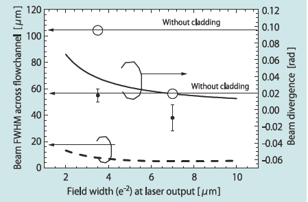
Fig. 11. Beam divergence and width across fl ow-channel. Solid line is numerical calculation and mark is experimental result.
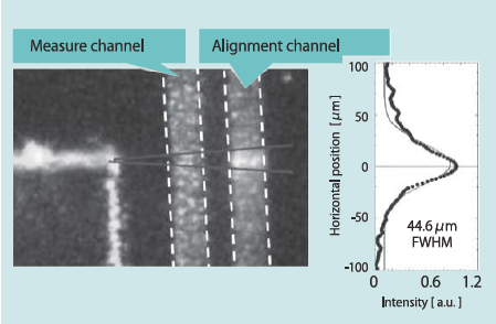
Fig. 12. HIDCI fluorescence image and beam intensity profile.
5.まとめ
全PMMAのモノリシックなマイクロ流路チップへのレーザーの組み込みプロトタイプを行い、レーザー蛍光実験を行った。さらにレーザーのアラインメントや構築向きの検討を行い、PDMSチップへの複合有機材料・光ファイバ導光を利用したチップ組み込みも行い、レーザー組み込みにおけるアラインメントやビーム広がりの最適化設計の検討と実験による問題確認を行った.今後はアラインメントの問題を解決し、具体的な信号検出実験に進むために、作製プロセスの改善と実験を行っていく。
プロフィール

興 雄司 (おき ゆうじ)
九州大学大学院
システム情報科学研究院 教授
(連絡先) 〒819-0395
福岡県福岡市西区元岡744
九州大学大学院
システム情報科学研究院
I&Eビジョナリー特別部門
九州大学伊都地区 ウエスト
2号館 606号室
TEL 092-802-3742
FAX 092-802-3731
E-mail:oki@ed.kyushu-u.ac.jp
- 経歴
- 1964年 12月19日生まれ
1987年 九州大学工学部電気工学科卒
1989年 九州大学大学院工学研究科電気工学専攻修士課程卒
1992年 同大学院工学研究科博士課程修了。工学博士同年より九州大学工学部に助手として在職
1995年 九州大学大学院システム情報科学研究科助教授
2000年 米国アリゾナ大光科学センター研究員
2001年3月 九州大学大学院システム情報科学研究院電子デバイス工学部門助教授
2008年4月 九州大学大学院システム情報科学研究院電子デバイス工学部門准教授
2008年4月 九州大学大学院システム情報科学研究院情報エレクトロニクス部門准教授
2013年2月 九州大学大学院システム情報科学研究院I&Eビジョナリー特別部門教授
2013年4月 同大学 分子システムデバイス国際リーダー教育センター教授 (兼任) - 現在の専門
- ○レーザー工学・レーザー分光特に色素・Ti:Sapphireなど可変波長レーザー、導波型レーザー、固体色素レー ザー、有機フォトダイオード、optofluidicsについて研究
○コンピューターにも通じ、TeXにおけるdviout開発、大学部局教育・研究システム開発などに携わる。
○2013年には応用物理学会シンポジウム「応用物理とMathematica」を実施 - 学会等役員
- ○応用物理学会、日本光学会、 レーザー学会、電気学会、OSA、EOS、IEEE、POS各会員
- 賞罰
- 1999年1月 レーザー学会学術講演会年次大会優秀発表賞
2003年4月 レーザー学会奨励賞
2008年11月 レーザー歯学会優秀発表賞
関連製品
論文を探す
今号では、医療診断の信頼性を実用レベルまで向上させることを目的とした「SPRセンサ向けセンサチップの開発」や排ガス処理に期待が寄せられている「常温無触媒脱硝法の開発」など、メディカルやライフサイエンス分野を中心に、6件の技術論文を掲載しました。
シリーズ「大学研究室を訪ねて」では、未来社会を支えるシステム情報科学の展開に挑む九州大学大学院・システム情報科学研究院の興(おき)先生をお訪ねし、今、話題の「光と有機物を利用したユビキタスセンシング技術の開発」をご紹介しております。
(2014年12月)