Compact High Power SMDEDCC Faimily(Compact High Power SMD)
The EDCC Family incorporates traditional high-power LED chips with a wide range of wavelength options, yet it achieves an impressive reduction in footprint of approximately 80% when compared to the previous small-sized EDC Family package.
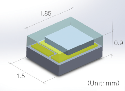
As a result, it offers a compact form factor (W1.5 x L1.85 x H0.9 mm) that closely resembles bare chips and is also compatible with CSP (Chip Scale Package) and other compact-sized packages.
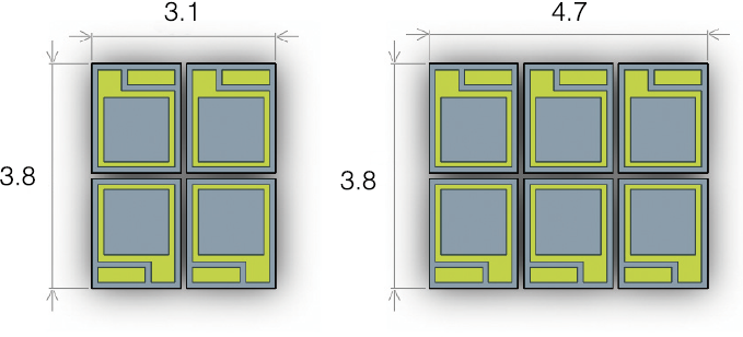
| Package area(mm) Example of LED placement |
 |
 |
|---|---|---|
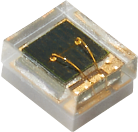
| Appearance |
|
|
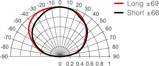
| Radiation Characteristics |
|
|
| 3D Data | Download | |
Key Features
・Compact-sized package, comparable to CSP and high-power LED chips, facilitating easy customization in an SMD-type LED format.
・Package design optimized for high-density integration.
Comparison with conventional products
| SMBB Flat | EDC Flat | EDCC | |
| Package area(mm) | 5.0×5.2 | 3.5×3.5 |
1.5×1.85
80% reduction compared to EDC Family
|
| Appearance |  |
 |
|
| SMBB850DS-1100 | EDC850DS-1100 | EDCC850DS-1100 | ||
| Vf[V]@1A | 3.2 | 3.2 | 3.2 | |
| Vfp[V]@5A* | 4.6 | 4.6 | 4.6 | |
| Po[W]@1A | 1.4 | 1.4 | 1.2 | |
| Po[W]@5A* | 5.6 | 5.6 | 5.3 | |
| Rthjs[K/W] | 9 | 11 | 21 | |
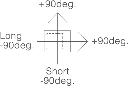
| φ1/2[deg.] | 64 | 66 | Long** | 69 |
| Short** | 69 | |||
** Radiation Characteristics of EDCC Package
Applications
・Machine Vision
・Optical Sorting
・Plant Growth
・Security
・Surveillance Cameras
・Optical Authentication
・Inspection Equipment
・Vital Sensing and more.
Minimum Order Quantity
For initial evaluation purposes, we will deal with less than MOQ only if we have it in stock. Please feel free to contact us.
Parts Numbering

(a) EDCC : Package Family Name
(b) 850 : Peak Wavelength. (unit:nm. From 365nm to 1,900nm)
(c) DS : Structure Type of LED Chips (Restrictive Option)
(d) 1 : Number of Chips (1: 1 Chip)
(e) 100 : LED Chip Dimension (100: 1,000um * 1,000um, 130: 1,300um * 1,300um)