Fundamental knowledge relating laser diode
Introduction to Optical-semiconductors
Optical-semiconductors refer to light-emitting devices that convert electricity into light, or, conversely, to photo sensors or light-receiving devices that convert light into electricity. Examples of optical semiconductors include light-emitting diodes (LEDs) and laser diodes (LDs) as light-emitting devices, and photodiodes, solar cells, and CMOS image sensors as photo sensors. In addition, optical semiconductors include optical modulation devices used in optical fiber communications and complex devices that combine these elements, such as photo couplers that transmit information between electrically isolated components.
Table. Examples of optical semiconductors
| Type | Specific examples of optical semiconductor devices |
| light-emitting devices | light-emitting diodes (LEDs) and laser diodes (LDs) |
| light-receiving devices | photodiodes, solar batteries, CMOS image sensors |
| Others | optical modulator, photo couplers, Optical switch |
Semiconductor materials have a unique energy value called the bandgap, which determines their light-receiving/emitting functions and the range of wavelengths that the material can be operated over.
In light-emitting devices, GaN, AlGaInP, GaAs, InGaAsP and other direct transition-type compound semiconductor materials are used. Also, both direct and indirect transition types can be used as semiconductor materials for photodetectors, with single-element semiconductor materials such as Si and Ge being mainly used in the visible to near-infrared wavelength range below 900 nm. For detecting and receiving light in the wavelength range over 1 μm, compound semiconductors based on InGaAs are mainly used.
USHIO INC. offers light-emitting diodes (LEDs) in the 365 nm to 1,300 nm wavelength range and laser diodes (LDs) in the 375 nm to 852 nm wavelength range.
Light-Emitting Devices
The basic structure of a semiconductor light-emitting diode has a PN junction diode structure using compound semiconductor materials. When a forward voltage is applied to a PN junction, current flows by the transfer of holes in the P-type semiconductor and electrons in the N-type semiconductor. These carriers are injected into the PN junction to generate energy equivalent to the bandgap energy of the semiconductor material when electrons and holes are recombined. If a direct bandgap semiconductor material is used at the junction, most of this energy is emitted as light. On the other hand, in the case of indirect bandgap semiconductors such as Si and Ge, the emission is very weak and is mostly converted to heat. Therefore, to achieve efficient light-emitting devices, direct bandgap semiconductor materials should be used.
Light-emitting diodes (LEDs)
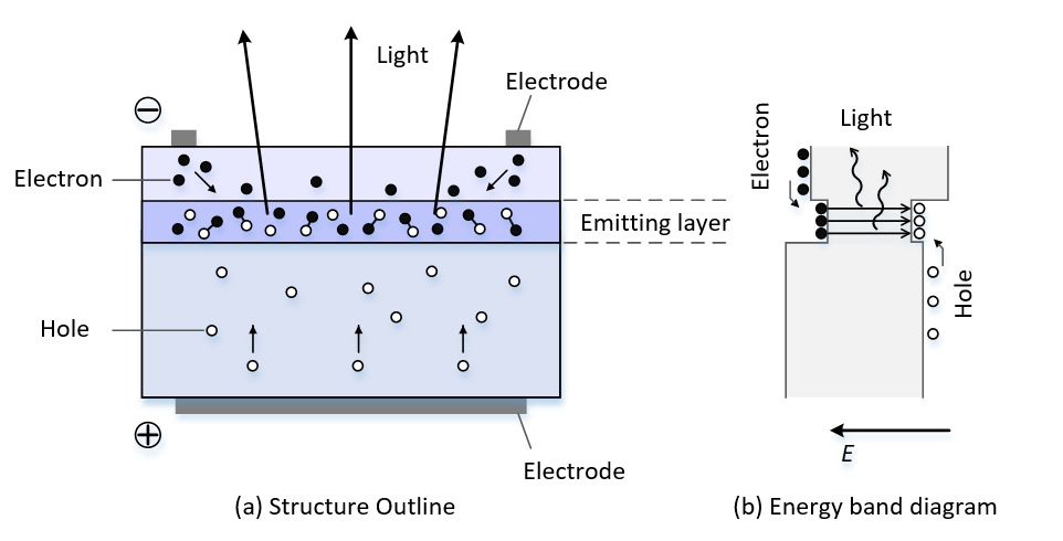
A light-emitting diode is an element with a PN junction diode structure that can efficiently extract the light generated by current injection. In order to increase the conversion efficiency of the current that flows in the device to the light, a double-hetero-structure is used at the PN junction. A hetero-structure is a junction in which different semiconductor materials are joined together; a PN junction of the same type of semiconductor is called a homo-junction. The double- hetero-structure consists of a P-type semiconductor layer and an N-type semiconductor layer, sandwiching an emitting layer with a smaller bandgap than the P-type and N-type semiconductor layers. This structure enables the emitting layer to work as a well or trap for the carriers, confining the carriers (holes and electrons, respectively) injected from the P-type and N-type layers to the emitting layer. The carriers accumulated in the emitting layer eventually recombine to generate light with an energy equivalent to the bandgap. This phenomenon is called spontaneous emission, as the carriers spontaneously recombine and emit light. The emission of light from each carrier recombination is an independent phenomenon and generates light with random phases. The light generated has a wavelength bandwidth depending on the energy distribution of the carriers accumulated in the emitting layer.
As described above, many of the semiconductor materials used in the emitting layers are direct bandgap semiconductors, which are commonly used for high-powered light-emitting diodes and are applied to optical communications due to their high-speed response which results from their short carrier life time.
However, it is also known that Indirect bandgap semiconductors can generate luminescence. By adding specific types of impurities into the emitting layer, the indirect transition type material GaP has been used for LEDs in the green to red range.
Laser Diode (LD)
LASER is an acronym for "Light Amplification by the Stimulated Emission of Radiation,".
While spontaneous emission results in a random phase of light, in stimulated emission, the interaction between a light wave and a carrier pair results in an amplification function where the carriers recombine to emit light of the same wavelength and phase as the original light. Therefore, the laser light is a single wavelength, phase-aligned and very intense light.
The basic structure of a laser diode is a PN junction diode with a double-hetero-structure, similar to a light-emitting diode (LED), but the following three conditions are required for laser oscillation.
(1) High optical gain
(2) Population inversion
(3) Resonator Structure
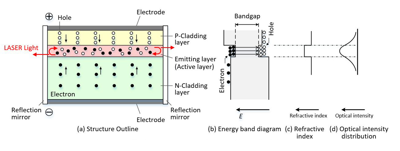
Firstly, (1) requires the emitting layer to be a direct bandgap semiconductor material with a structure that enables direct emission by recombination of carriers. Secondly, while light emission by spontaneous emission begins when a current is applied to the device and carriers are injected into the emitting layer, light absorption also occurs in the emitting layer by a process opposite to light emission. When the drive current of the device is low and the carrier density of the emitting layer is low, absorption is more dominant than emission. As the drive current is increased, more electrons and holes are accumulated in the emitting layer , eventually resulting in an amplification effect through stimulated emission, a state which is referred to as “population inversion” (2). In order to make a device work as a laser, a resonator structure (3) is also required. The light amplified inside the device is confined in a resonator structure and amplified by multiple passes through the gain region to achieve laser oscillation. The simplest resonator structure consists of two reflective mirrors facing each other. To obtain efficient stimulated emission, it is necessary to concentrate the light into the emitting layer, so that it can interact with the confineds the carrier. Fortunately the double-hetero structure described above makes it possible to confine the light to the emitting layer.
In general, the refractive index of semiconductor materials tends to be higher as the bandgap becomes smaller in the same type of material. At the same time, light tends to gather in places with a high refractive index. In the double-hetero structure, the band gap of the emitting layer is small and the refractive index is high, which confines the light as well as the carriers, enabling efficient laser oscillation operation.
In laser technical terms, the emitting layer, where laser light is generated by carrier recombination, is called the active layer, and the layers on either side of the active layer are called the cladding layers. This is because, in an optical waveguide structure that confines light and allows it to propagate like an optical fiber, the layer that confines the light with a high refractive index is called a core and the outer layer with a low refractive index is called a cladding, which means that a semiconductor laser also has the function of an optical waveguide.
Features of Laser Diodes
There are four main features of laser diodes.
- Single-wavelength coherent light
- Compact and lightweight
- Low power consumption and high efficiency
- High-speed response and direct modulation are possible.
The monochromaticity is one of the unique features of laser. While sunlight and other light sources contain various wavelengths of light and exhibit a very broad spectrum, light-emitting diodes have a relatively narrow spectrum. In contrast, a laser that resonates and amplifies light of a specific wavelength can produce a single wavelength of light. For example, when displaying images, various colors are represented by the three primary colors of RGB (Red, Green, Blue). In general, the light from a white light source such as a lamp or white LED is separated into the three primary colors of RGB using a filter to control the display color. However, with this method, each RGB color has a certain wavelength bandwidth, and not all possible colors can be represented by superimposing them together. Alternatively, the use of a tri-color RGB laser light source can produce images that are more vivid and have superior color saturation and wider color gamut.
-
(a) Sunlight (daylight) -
(b) Xenon Arc lamp -
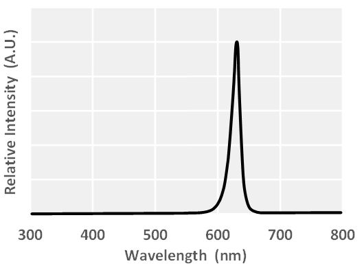
(c) Light-emitting diode (630nm) -
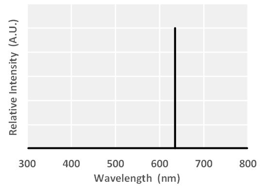
(d) Laser Diode(630nm)
Fig. Comparison of Spectrum of Various Light Sources
In addition, its coherent light makes it possible to use laser light in a variety of applications. One of its most significant features is its high directionality and is able to focus down to the diffraction limit with an optical system such as a lens. For example, in the case of DVD and BD optical discs, a laser beam is focused on a tiny spot with a diameter of 100 to several hundred nm to read the information on the optical disc, and the reflected light returned from the disc is detected by interference elements and converted into an electrical signal. It is also used in sensing technology to precisely measure the distance and direction to an object by scanning a narrowly focused laser beam.
Among several types of laser light sources, the laser diode has the outstanding feature of being compact and lightweight. The size of the laser chip itself ranges from 100 micrometers to 3 millimeters, and the packages in which the laser chip is embedded are also very small, typically only a few millimeters. In contrast, He-Ne lasers, a typical gas laser, are extremely large, ranging from 20 cm to 1 m. Needless to say, this is one of the factors that has made it possible to easily integrate diode laser light sources into various types of equipment.
Table. Examples of laser types and features
| Type | Wavelength (μm) | Optical Output Power (W) | Efficiency (%) | ||
|---|---|---|---|---|---|
| Diode laser | InGaN | 0.37 ~ 0.53 | CW | 5W | 40 |
| AlGaInP | 0.63 ~ 0.70 | CW | 3W | 40 | |
| Solid-state laser | Ti Sapphire | 0.8 | Pulse | 1W | 0.1 |
| YAG | 1.06 | CW | 400W | 3 | |
| Liquid laser | Dye laser | 0.3 ~ 0.9 | Pulse | 100W | 0.3 |
| Gas laser | He-Ne | 0.633 | CW | 0.05W | 1 |
| Ar | 0.488, 0.514 | CW | 1W | 0.1 | |
| CO2 | 10.6 | CW | 10kW | 20 | |
In terms of laser performance, laser diodes are characterized by low power consumption, high efficiency, and direct modulation. The drive voltage of a laser diode is about 1 to 5 V, which is low enough to run on batteries, and can be driven by a small current. As for the efficiency of converting input power into laser light output, laser diode operate by current injection and use the phenomenon of direct conversion of electricity into light, making it easier to increase the conversion efficiency. On the other hand, other types of lasers, such as gas and solid-state lasers, have an inversion distribution that is obtained by pumping the laser medium by optical excitation or radio-frequency discharge, which results in an unavoidable loss of energy and relatively lower efficiency. In addition, a laser diode is driven by current injection, which makes it possible to control the optical output simply by modulating the amount of drive current, and thus enables direct modulation of optical output. At the same time, since the photon lifetime in the semiconductor material is very short, and the carrier lifetime is also very short, a fast response time of about 1 ns is possible.
Semiconductor Materials
Compound semiconductor materials, especially those of the III-V group, which are a combination of group III and V elements, are widely used in light-emitting devices. This is because the bandgap of compound semiconductor materials can be changed by composition of materials (composition ratio), and they can become the direct bandgap semiconductors required for light-emitting devices.
The table below shows examples of compound semiconductor materials and emission wavelengths for use in light-emitting devices (especially laser diodes).
Table. Semiconductor Materials and Wavelengths
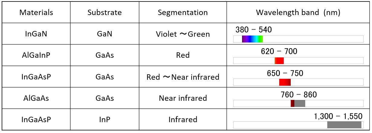
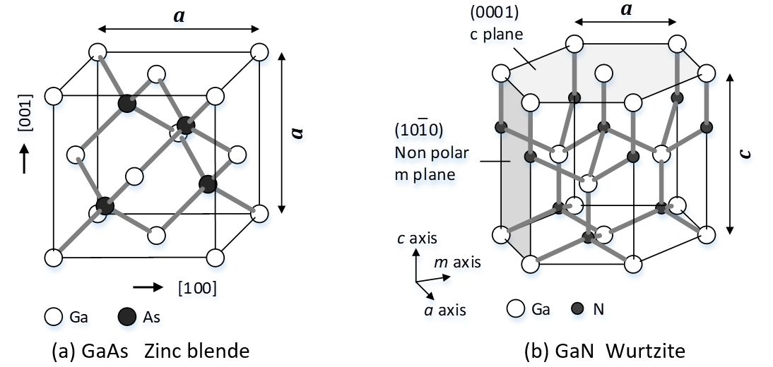
These semiconductor materials have a crystalline structure in which the constituent elements are arranged in an orderly manner, and the semiconductor materials that make up the device are formed by crystal growth on a substrate with a consistent crystal lattice (called epitaxial growth). Binary semiconductor materials (GaN, GaAs, InP, etc.), which are relatively easy to fabricate, are generally used as semiconductor substrates.
For example, GaN has a wurtzite crystal structure and GaAs has a Zinc blende structure, and the composition of the semiconductor materials to be formed on these substrate crystals must be adjusted to have the same crystal structure and lattice constant as the substrate crystals.
The compound semiconductor has a strong cleavage property. Another reason why they are used in semiconductor lasers is that they can be split along a single crystal plane by cleavage to form a very flat surface that can be used to form the mirror surface of a laser diode.
The following explanation is based on the example of an AlGaInP semiconductor laser that emits light in the red region. First of all, AlGaInP quaternary compound is a semiconductor material composed of three binary compounds in a fixed ratio. The bandgap and lattice constants are determined by the ratio of the three group III elements in the region with AlP, GaP, and InP at the vertices in the figure below. Among these binary compounds, AlP and GaP have almost the same lattice constant, and the lattice constant of AlGaInP quaternary is determined by the ratio of the composition ratio of In to the sum of the composition ratios of Al and Ga, and thus the compositional constants of AlGaInP crystal are usually described in the form of (AlxGa1-x)0.5In0.5P. The cladding layer of the laser waveguide confinement structure requires a material with a large band gap, so AlGaInP compounds with an Al composition of 0.7-1.0 are often used. The active layer is often composed of GaInP compounds, and the multiple quantum well (MQW) structure, in which nanometer-order thin films are piled up, controls the oscillation wavelength by changing the bandgap resulting from the quantum size effect.
As described above, in the crystal growth of the semiconductor materials that constitute a laser device, lattice-matched crystal materials are required to be formed on the semiconductor substrate. However, in thin-film structures such as the active layer in the MQW structure, crystalline materials with lattice constant deviations can be used intentionally, as long as the strain energy due to lattice distortions does not exceed a definite value. In recent years, such strained quantum well structures have been widely used to control the oscillation wavelength and improve the characteristics of lasers.
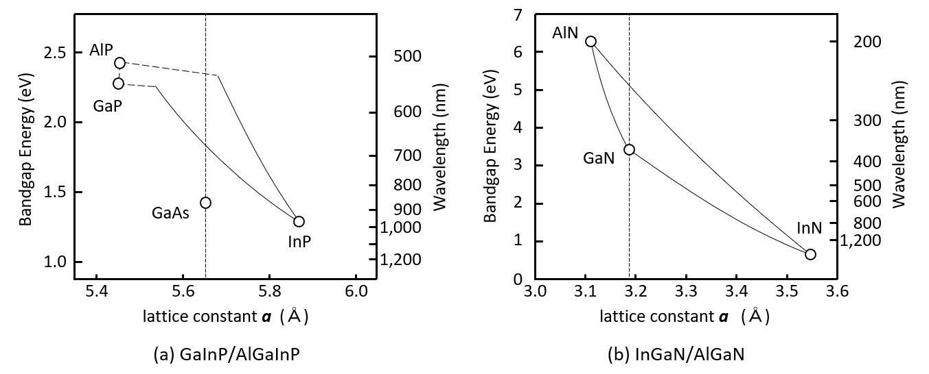
GaN-based lasers, which oscillate in the blue-violet to green region, generally use AlGaN for the cladding layer and InGaN for the active layer, and the bandgap and lattice constants are controlled by adjusting the composition of group III Al, Ga, and In in the same way as described above. In these materials, the lattice constant of the AlGaN cladding layer and the InGaN active layer is different from the GaN of the original semiconductor substrate, and the structure has an inherent strain stress.
In particular, there is a problem of piezoelectric polarization induced by lattice misalignment with GaN (creating localized distributions of electrons and holes in the InGaN active layer, resulting in reduced luminescence efficiency) and difficulty in the growth of large In-rich InGaN layers. To solve these problems, investigations of lasers using non-polar and semi-polar GaN substrates and the development of new crystal growth techniques are in progress.