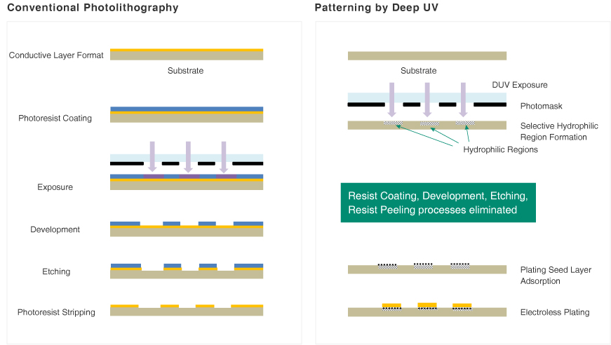
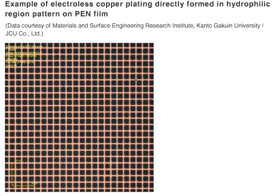
Non-electrolytic copper plating pattern by surface modification patterning
Selective creation of hydrophilic region through photomasks of resin film, etc. The non-electrolytic copper plating pattern is formed after adsorption by just the hydrophilic region of the plating seed layer. Conductors can be formed without resorting to photoresist patterning.