光技術情報誌「ライトエッジ」No.31
2008.6 25th International Conference of Photopolymer Science and Technology (ICPST-25)
(2008年10月)
A Study of Photoresist Pattern Freezing for Double Imaging
using 172nm VUV Flood Exposure
Masanori Yamaguchi,* Thomas Wallow,‡ Yohei Yamada,* Ryoung-Han Kim,‡
Jongwook Kye,‡ Harry J. Levinson‡
*Ushio Incorporated, 1194 Sazuchi, Bessho-cho, Himeji, Hyogo Prefecture JAPAN 6710224
‡Advanced Micro Devices, One AMD Place, Sunnyvale CA USA 94088
m.yamaguchi@ushio.cajp,tom.wallow@amd.com
Numerous alternate processes are under industry wide evaluation as simplifications to current double patterning methods. Reduction in process complexity and cost may be achieved by use of track-based photoresist stabilization methods that eliminate one etch step by allowing a second resist to be patterned over a first resist pattern. Here, we describe studies of 172nm flood UV exposure as one example of a resist stabilization method. When properly implemented, we observe that 172nm stabilization allows superior retention of photoresist profiles vs. longer wavelength UV treatment. For the commercial 193nm photoresist studied, judicious choice of 172nm dose and subsequent bake is required for pattern stabilization to second resist processing. FT-IR studies indicate that distinct chemical processes occur during 172nm flood exposure and subsequent bake: 172nm flood exposure appears to cause selective decarboxylation of lactones present in the photoresist, while baking leads to photoacid-mediated loss of blocking groups and other processes that are not conclusively characterized at present. At 800 mJ/cm2 172nm dose, resist patterns are sufficiently stabilized to prevent reflow in the subsequent bake. Approximately 25% volumetric shrinkage accompanies 172nm stabilization. This shrinkage is manifested as controllable CD trimming and thickness loss as well as 3-dimensional resist pattern distortion including line-end tilting and corner bowing. At insufficient 172nm cure doses, photoresist reflow occurs during the subsequent stabilizing bake. 3-Dimensional resist pattern distortions are dramatically larger under these conditions. These findings indicate that shrinkage control during any stabilizing process is a critical factor in resist design for simplified double patterning methods.
Keywords
Double patterning, resist stabilization, pattern distortion, 172nm cure
1. Introduction
Double patterning methods that simplify integration of lithographic and etch processes are of growing importance due to their potential for improved manufacturing throughput and cost savings. Increasing efforts in this area center on double imaging processes in which two or more independent lithographic patterns are generated in sequentially applied resist films, then transferred in a single etch step (fig. 1)[1-15].
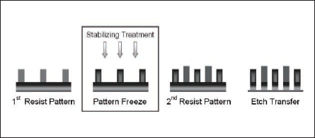
Fig.1 : Double imaging schematic. Application and patterning of a second resist film over a pre-existing, first resist pattern requires a stabilizing treatment.
Stabilization of the first photoresist pattern to processing of the second resist pattern is necessary in double imaging. Without stabilization, the first resist pattern will swell or dissolve on application of the second resist film, or undergo additional exposure and development during the patterning of the second resist. Numerous chemical[3,6,9,10-13],photochemical[1-4,14],thermal[8], and ion-beam[5,7,15] stabilization methods have been recently described. Key issues for double imaging remain to be resolved, including applicability to regular and irregular resist structures, scalability from 45 nm to 22 nm technology nodes, and track-based process complexity. The first two of these issues specifically require detailed assessment and understanding of all aspects of resist pattern changes that occur during double imaging.
In this presentation, we report on resist shrinkage and distortion during stabilization in the context of double patterning. We have chosen to focus on 172nm stabilization due to its relative simplicity as well as promising initial demonstrations of superior profile retention in 193nm resists using 172nm stabilization vs. longer wavelength UV stabilization (fig. 2).
Studies reported here allow us to more accurately assess implementation strategies for double imaging in future logic lithography technology nodes. Additionally, these results indicate potential overall resist design and stabilization process optimization strategies that will aid in development of more robust double imaging methods.
2. Experimental
Patterning evaluations were conducted in a R&D fab cleanroom environment using a prototype 193 nm stepper. Following processing, wafers were double-bagged in nitrogen-purged, sealed, metal foil-lined plastic bags for transfer to the 172nm cure processing facility.
The 172nm cure chamber was designed for highly reproducible irradiation. It allows process evaluation and development under controlled environmental conditions and is configured with in-situ monitoring probes to achieve uniform process conditions. All wafer handling was carried out under yellow lights in an R&D cleanroom.
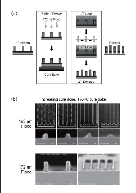
Fig.2: (a) Double imaging schematic using 172nm stabilization. In this study, the 172nm exposure is followed by a post-flood exposure cure bake to fully stabilize the first resist pattern. (b) Resist profile comparison following 193nm and 172nm stabilization. Images are for resist features that have been stabilized by flood exposure and 170t bake, then re-exposed at 193nm and re-developed to mimic parts of the second resist process. For 193 nm stabilization, swelling during second development cannot be suppressed without causing resist reflow. 172 nm stabilization can suppress swelling without causing reflow.
A commercial 193nm resist was chosen as the focus of these studies based on preliminary screening of several resist candidates. We note that response to pattern freezing steps (both 172nm flood exposure and post-flood bake) varies widely among commercially available resists. Films were coated at 200nm thickness on a reflectivity-optimized commercial BARC. All standard process steps used supplier-recommended conditions.
FT-IR, XPS, and VUV spectroscopy were carried out using commercially available instrumentation on resist films cast onto appropriate substrates. Commercial analytical SEMs were used for all pattern deformation studies. Resist patterns shown in Tilt-SEM images in figs. 2, 4, 7 and 8 were metal coated. Other samples were not metal coated, and low current and voltage SEM conditions were used to minimize resist shrinkage effects.
3. Results and Discussion
3.1 172nm resist stabilization: shrinkage and CD trimming
In order to fully stabilize the specific resist studied here to 2nd resist processing in double imaging, a post-172nm exposure stabilizing bake is required. However, for purposes of fundamental understanding, we examined the role of 172nm exposure independent of a subsequent hardbake as well. At 7.2 eV, 172nm photons possess sufficient energy to cause non-selective homolytic bond cleavage in organic materials. Substantial materials property changes should result from 172nm exposure alone.
Irradiation or other stabilization of photoresists has been frequently described as a method for CD trimming[16-18]. Fig. 3a shows that 172nm irradiation produces controlled dose-dependent CD changes in line/space patterns. Exposure latitude curve fits were employed to measure average ΔCD vs. 172nm dose values. Similar measurements were carried out for target half-pitches ranging from 130 to 150nm in both darkfield and brightfield environments. Results are plotted in fig. 3b. The CD trimming produced by 172nm irradiation showed no systematic dependences on CD, half-pitch, or pattern density in our experiments. This allowed us to fit a master curve to all CD shrinkage data. We note that 172nm-mediated shrinkage is initially strongly dose dependent, but begins to saturate at doses above 800 mJ/cm2. At 800 mJ/cm2, stabilization results in 17 +/—4nm CD trim: assuming isotropic feature shrinkage, this corresponds to ~25% volumetric shrinkage. Other UV cure stabilization methods show comparable or larger volumetric shrinkage, depending on material and process implementation[16-18].
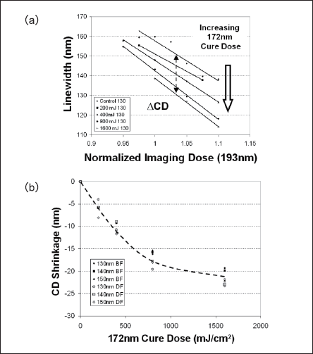
Fig.3:CD trimming during 172nm exposure. (a) ΔCD appears independent of pre-172nm exposure CD for feature sizes studied here. Thus, exposure latitude plots can be used to determine ΔCD as a function of 172nm exposure.
(b) ΔCD vs. 172nm cure dose for a range of line/space target dimensions.
3.2 3-Dimensional pattern distortions
Numerous previous reports on resist stabilization have noted that volumetric shrinkage effects can produce feature-specific 3-dimensional pattern distortions[13-21]. For double imaging generality, any pattern distortions need to be assessed for severity and possible correction within a given set of design rule constraints. To date, the majority of double imaging implementations have been demonstrated using highly regular structures such as pitch-split line/space arrays or crossed-grid contact hole arrays. Successful use in more complex patterns containing line ends or corners will expand the utility of double imaging. In order to gain a preliminary understanding of 3-dimensional distortions during 172nm stabilization, we focused on behavior of line ends and 90 degree elbows.
Fig. 4 illustrates the behavior of line ends following 172nm stabilization. As 172nm dose increases, line end tilt becomes more pronounced. In order to analyze these images semi-quantitatively, we have applied a simple geometric SEM tilt perspective correction. We recognize that SEM image distortions may not be fully compensated for in this manner. Nevertheless, this method allows much better comparison of dose-dependent line end tilting than can be inferred from top-down SEM analysis. At 800 mJ/cm2, line ends are tilted by approximately 25 degrees.
This behavior is expected for free-standing resist beams undergoing volumetric shrinkage: stresses will be most pronounced parallel to the long beam axis and will be most readily relieved at line ends. Kim et al[17]. reported line-end pullback by top-down SEM measurement of resist features cured with 172nm light, but did not associate pullback with line-end tilting. Analogous effects have been observed in a bilayer reflow process, where stress-induced necking of narrow resist beams that connect larger resist islands may be exploited for CD trimming[21].
Several patterning and pattern transfer challenges may arise from line-end tilting. Tilted line ends will complicate metrology and SEM analysis, both during routine process monitoring and OPC development. Careful SEM image analysis of top and bottom resist contours is needed to accurately capture tilt impact on line-end placement tolerances. Etch transfer of tilted line ends may produce distortions arising from the poor local sidewall angle.
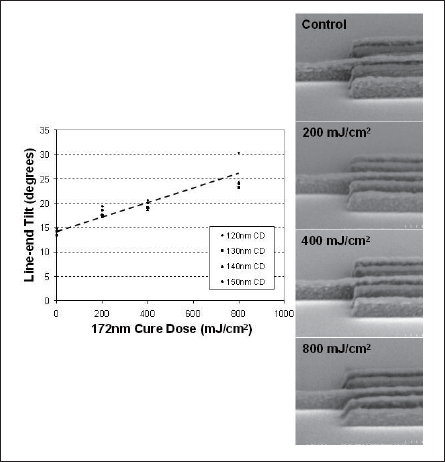
Fig.4:Shrinkage distortion at line ends as a function of 172nm dose. 130nm half-pitch line ends are shown.
Pattern distortions are also seen at 90 degree elbows. In this resist beam geometry, stresses generated in perpendicular beams must be relieved (Fig. 5). We have carried out analysis of the resulting corner bowing and positional displacement using both top-down and tilt SEM images.
Fig. 5 details the top-down SEM methodology used to infer corner displacement arising from corner bowing. Along a diagonal cut line (ii), corner displacement due to shrinkage can be estimated from the inner and outer corner positions of elbows referenced to the corner position of the original pre-stabilized resist pattern. In order to generate the positional reference, we extrapolate pre-shrink line contours to yield a point on the diagonal cut-line that corresponds to the idealized outer mask elbow corner. ΔCD for lines far from the corner (cut line (i), for instance) can be determined for all stabilization conditions. Since trimming occurs equally on both line edges, ΔCD can be used to recover the original pre-stabilization reference location for trimmed patterns. Position and displacement of both inner and outer elbow corners can thus be determined consistently for all stabilization conditions. Other geometric approaches are equally valid; the method used here proved convenient given readily available image line-edge analysis software[22].
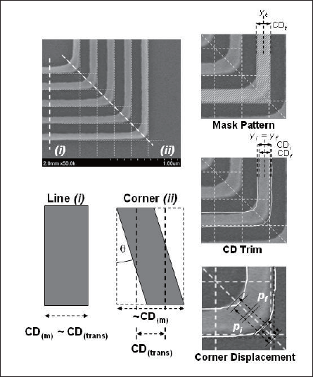
Fig.5:Comparison of resist shrinkage effects along lines and in feature corners. Cut lines (i) and (ii) define pattern positions for lines and corners, respectively.
Corner bowing was also examined using tilt-SEM. For these experiments, the same geometric perspective corrections as described for fig. 4 were used. Outer elbow corner tilt angles were measured at 45 degree angles from the long resist line axes (fig. 6.)
Corner tilt angles from tilt-SEM can be used to estimate corner positional displacement. Estimates generated in this way are quantitatively much larger than estimates from top-down SEM, but show comparable dose dependence behavior. Differences in methods will require additional evaluations, such as AFM profiling, to resolve.
Outer corner tilt vs. 172nm stabilizing dose for elbow features ranging in line/space half-pitch from 120 to 150nm is shown in fig. 7. Corner tilt increases with stabilizing dose, but shows little dependence on CD or pitch for the features studied here.
Corner bowing presents the same patterning and pattern transfer challenges that were discussed previously for line-end tilting: careful assessment of impacts on metrology, OPC development, and etch transfer fidelity is needed. Previous investigations have described corner distortions arising during resist cure, but have not characterized these in detail[16,17].
For insufficient 172nm doses, the resist is not sufficiently stabilized to developer and can undergo swelling or dissolution, and is also susceptible to reflow during the stabilizing bake. Fig. 8 demonstrates that both line-end tilt and corner bowing can be drastically more pronounced in the presence of resist reflow. Post-development reflow bakes have been evaluated as methods for smoothing line edge roughness[23,24]: results shown in fig. 8 suggest care must be taken if these methods are used for complex resist patterns.
When both 172nm exposure and subsequent bake conditions are optimized, resist profile retention following proxy second resist processing steps is possible. Fig. 9 shows resist profiles following 800 mJ/cm2 172nm irradiation, 170°C stabilizing bake, and second development. Features retain surface roughness similar to control samples, indicating that no reflow or significant swelling has occurred in the course of these process steps.
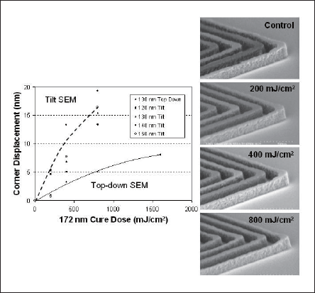
Fig.6: Comparison of resist corner displacement measurements. Overall trends are the same, but displacements inferred from tilt SEM are much larger than those inferred from top-down SEM measurements.
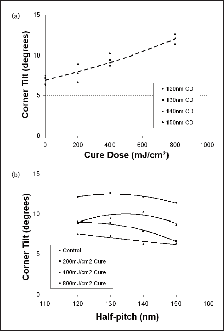
Fig.7:Resist corner tilt as inferred from tilt-SEM analysis.
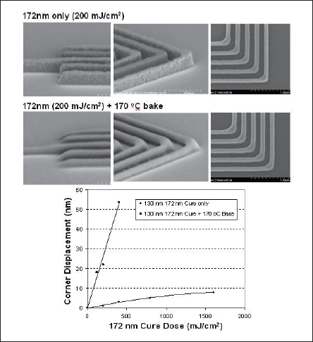
Fig.8:lmpact of resist reflow on profiles, line-end tilt, and corner displacement.
3.3 172nm exposure of unpatterned resist films.
Unpatterned 200nm thick photoresist films were subjected to a range of 172nm exposure doses as well as subsequent bakes. Film changes were characterized by FT-IR, XPS, and VUV spectrometry.
FT- IR interpretation of the carbonyl stretch region (1700 to 1800 cm-1) indicates that the photoresist contains a variety of linear ester groups (-1720 cm-1) as well as an alicyclic lactone, which is well resolved near 1800 cm-1. The majority of 193nm photoresist polymers are well known to contain complex methacrylate copolymers. These copolymers in turn incorporate at least three monomer types: lactone-bearing monomers are one widely used group whose function is to impart crucial physical and interfacial properties to photoresists. A full spectral analysis is inappropriate given this compositional complexity, and we will focus only on key chemical transformations.
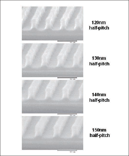
Fig.9: Cross-sectional profiles of resist features following 800mJ/cm2 172nm exposure,170°C bake,and proxy 2nd development. Under these conditions, resist profiles are successfully preserved.
Following 172nm irradiation, a variety of dose-dependent changes can be seen, particularly in the carbonyl stretch region (fig. 10). Carbonyl loss occurs for all ester and lactone groups, but is enhanced for the lactone. More than 80% of the lactone groups initially present appear to be transformed or removed by 800 mJ/cm2 irradiation. In contrast, less than 20% of linear ester carbonyls are transformed or removed at the same dose. Peak shift with increasing dose for the complex linear ester peak from 1723 cm-1 to 1715cm-1 suggests that differences in reactivity to 172nm light exist among the esters represented in this peak. These differences appear less pronounced than for the lactone.
Comparison of films irradiated with 172nm light, then baked at 170°C, indicates that transformation of the lactone occurs predominantly during irradiation: following bake, ratios of lactone to ester carbonyl stretch intensities remain approximately constant for all 172nm doses. Substantial decreases in C-H stretch and various C-C vibrational modes indicate that hydrocarbon loss occurs during the subsequent bake: we attribute this to removal of blocking groups cleaved by photoacids produced during 172nm exposure.
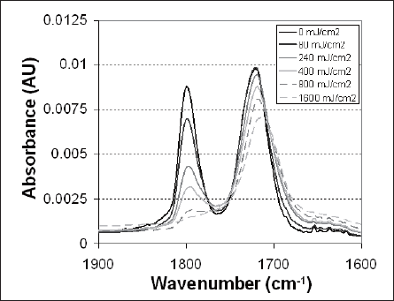
Fig.10:FT-IR monitoring of resist decarboxylation during 172nm stabilization. The peak at 1720 cm-1 represents linear esters in the resist; the peak at 1800 cm-1 represents an alicyclic lactone.
XPS analysis of films exposed to 172nm light reveals systematic loss of oxygen with increasing dose. Before exposure, resist films contain 18% (atom percent) oxygen near the film surface. 172nm exposure at 1600 mJ/cm2 reduces oxygen concentration to approximately 12.5%: enrichment of atomic carbon content accompanies oxygen loss. Cls carbon bonding changes near 286 eV indicate predominant O-C=O loss as well as some C-O loss. Subsequent 170°C baking does not produce conclusive additional changes at the resist surface.
VUV spectroscopy of films exposed to 172nm light showed gradual increase in absorbance near 195nm as well as growth of a longer wavelength tail to beyond 250nm. This result is consistent with buildup of chromophores resulting from decarboxylation and other elimination reactions, but does not provide additional specific insight into the chemical structure of the irradiated films.
These observations are in overall good agreement with previously observed 193nm resist reactivity during exposure to UV light or other energetic particles, and suggest that lactone and ester photochemical decarboxylation play a large role during resist stabilization. Many of the photoresist stabilizing treatments currently under consideration for double imaging have been previously considered for other resist process enhancements including etch resistance improvement [19], ion implant improvement [16,17], and CD trimming [16-18]. These reports allow additional interpretation of the resist stabilization studies described here. Decarboxylation has been widely documented as a predominant chemical transformation during exposure of 193nm photoresists to UV light [16,17,21,25,26], electron bombardment [19,28-31], and ion bombardment [10,27]. While many polymer platforms have been studied, including lactone-containing materials, we are not aware of other reports showing the degree of selectivity for lactone decarboxylation that is observed in this study.
Whether lactone selectivity is fundamentally related to pattern freezing capability remains to be determined. Recently, Ito and coworkers[32] showed that alicyclic lactone monomers possess previously unrecognized reactivity in photoresist films. In particular, lactones are basic enough to interact with both photoacids and blocking group fragments released during chemical amplification. In the case of the latter, covalent reattachment of blocking group fragments to the photoresist polymer can result. Similar reaction pathways may aid in polymer stabilization during baking following 172nm irradiation, but it is not clear that these pathways are effective during the room temperature 172nm irradiation itself, where photoacid-mediated blocking group cleavage is not likely to occur to any significant extent.
Additional fundamental studies of photoresist modifications occurring during and following stabilizing treatment may contribute strongly to the development and improvement of double imaging. We note that pattern distortions characterized in this work are likely to restrict use of double imaging to very regular patterns such as pitch splitting and crossed-grid contact holes. Accommodation of distortions through design rule modifications has been previously discussed [5,18], and provides one potential route to more general adoption of double imaging. Further advances are likely to come from both process-based refinement and resist materials advances. Resist materials that are less susceptible to shrinkage, require lower stabilization doses, and undergo VUV-light mediated stabilization to all second resist process steps without requiring a subsequent bake would offer substantial advantages.
4. Conclusion
Resist stabilization using 172nm light appears to have unique potential for double imaging applications. Under optimized conditions, a 172nm cure is capable of superior resist profile retention vs. longer wavelength UV cures. We have studied the 172nm stabilization process in detail in order to assess the general utility of cure-based double imaging approaches. 172nm irradiation results in selective decarboxylation of lactone esters as well as less selective decarboxylation of linear esters present in the resist. Decarboxylation and associated processes result in dose-dependent shrinkage of the resist. For line/space patterns, the resulting CD trimming is well behaved. Resist distortion effects in more complex geometries include line-tilt and elbow corner bowing. At 25% volumetric shrinkage, these appear problematic, and may limit application of cure-based resist stabilization processes to very regular structures. If stabilizing doses that result in lower volumetric shrinkage are used, distortions become more acceptable, but currently used resists do not withstand additional resist processing steps under these conditions.
Acknowledgments
The authors gladly acknowledge and are thankful for lithographic and SEM technical assistance from Hoa Truong, Bob Allen, and the staff at the IBM Almaden Reseach Center; lithographic assistance from Alden Acheta (Spansion, LLC); FT-IR analysis from Jeremias Romero (Spansion, LLC); and thin film analysis from Hiroshi Sugahara, Akiko Shinohara, and Michiko Morooka (Ushio, Inc.) We would also like to thank Toru Fujinami for helpful discussions.