Investigating the fine line lithography process on the large-size organic panels for advanced packaging and development
Naoya Sohara, Ryotaro Takahashi, Hirosuke Takamatsu
USHIO INC,1-90 Komakado,Gotenba city, Shizuoka pref, Japan
概要
半導体のコスト・性能の向上は、これまで主に微細化によって進められてきた。ただし、光源の短波長化やマルチパターニングに伴い、微細化のコスト面の増大が問題となっている。
そのために、性能向上の別の手段として、様々なチップを1つのパッケージ上に乗せてシステムとしての性能を上げる“ Heterogeneous Integration” が開発されてきた。例えば、機械学習に応用されるHPCの性能向上のために、Silicon-interposer(2.5D)で演算チップやメモリーチップを統合したSoCが開発されている。この先端パッケージに利用されている露光装置には、微細配線の解像性能と、大面積による高生産性の両面が求められている。
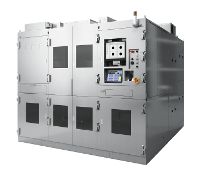
本論文・発表では、最新の□500mmの基板向けパネル露光装置を使い、各種DFRの露光結果を用いて、解像力を検証する。そして、最後に、露光光学系とプロセスの観点から、次世代の露光装置とプロセスについて述べる。
Improvements in the cost and performance of semiconductors have been driven primarily by miniaturization. However, as light sources have become shorter wavelengths and multi-patterning has increased, the cost aspect of miniaturization has become a problem.
As another means of improving performance, "Heterogeneous Integration" has been developed, in which various chips are placed on a single package to improve system performance. For example, a silicon-interposer (2.5D) SoC with integrated arithmetic and memory chips has been developed to improve the performance of HPC for machine learning. The exposure systems used for these advanced packages are required to have both resolution performance for fine wiring and high productivity due to the large area.
In this paper/presentation, the resolving power will be verified using the latest panel exposure system for □500mm substrates and the results of various DFR exposures. And finally, the next generation of exposure systems and processes are described from the perspective of exposure optics and processes.
Copyright © USHIO INC. All Rights Reserved