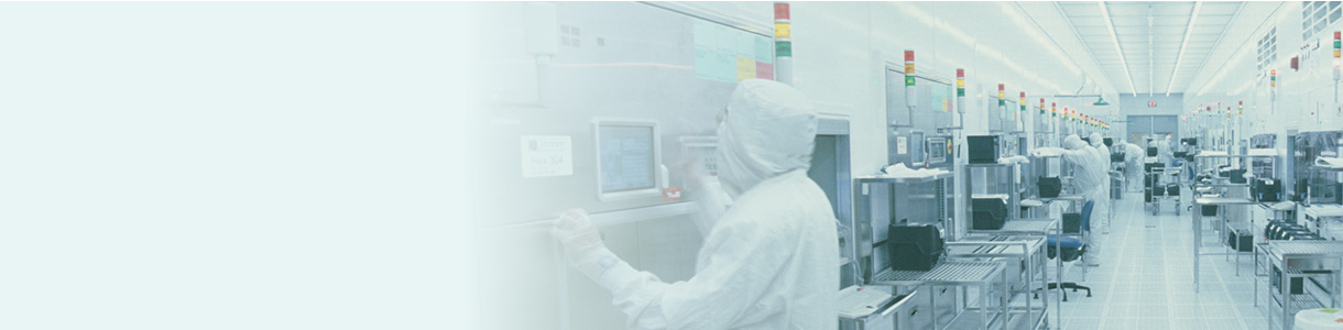
Implementation examples
Here too, Ushio Light.
Here too, Ushio Light.
As illumination, and as energy.
We introduce a variety of solutions made possible by Ushio Light.
Functions and applications
- All
-

Nano Imprint Mold Cleanging
-
Wafer 표면상의 유기물 제거
-
산화막 성막
-

Gold nanoparticle patterning
-

AHAPS-SAM patterning
-

SAM patterning
-

Surface modification
-

Greater hydrophilicity (wettability and contact angle reduction), improved adhesion
-

Precision cleaning and residue removal; (damage-free UV ashing)
-

Room temperature bonding through surface activation
-

Ushio light and manufacturing processes of flat panel displays
-

Ushio light and semiconductor manufacturing processes
-

Ushio light and manufacture of touch panels
-

Printable patterning
-

VUV patterning applications to organic transistors (transistor leads)
-

Non-electrolytic copper plating pattern by photosensitive material patterning
-

Non-electrolytic copper plating pattern by surface modification patterning
-

Sintering of Cu nanoink light by flash lamp
-

Example of heat resistance improvement
-

Ushio UV curing
-

Liquid crystal display manufacturing process innovation 1: One drop fill (ODF)
-

Liquid crystal display manufacturing process innovation 2: Photoalignment technology