Responding to Photoelectronic Fusion - Ushio Develops New Interference Lithography Equipment with Pitch Compensation Optics and Phase Shift Formation Function
Ushio Inc. (Head office: Tokyo, President and CEO: Takabumi Asahi, hereafter "Ushio") has successfully developed new interference lithography equipment that achieves an interference fringe pitch accuracy of 0.01nm and realizes the formation of phase shift structures. The product is scheduled to be launched in the spring of 2027.
The amount of power handled in data centers is becoming an issue due to increased competition in generative AI (Artificial Intelligence), and there are high expectations for photoelectronic fusion*. Laser light sources used for photoelectronic fusion are called DFB-Laser diodes (distributed feedback lasers) with diffraction gratings in the waveguide, and demand is growing rapidly. However, the productivity of EB (electron beam lithography) equipment used to form diffraction gratings is low and supply has not kept pace. It is widely known that interference exposure technology has the potential to solve the low productivity of EB, but has not yet been applied to mass production due to the following three issues.
(1) Unable to obtain stable exposure quality
(2) Low pitch accuracy
(3) Phase shift structure cannot be formed
This time, Ushio proposes a new interference lithography equipment that solves the above three issues.
(1) Excellent exposure stability with DPSS laser and KrF photoresist
Conventional interference lithography equipment uses a gas laser as the light source and a photoresist having strong linear property, resulting in a problem of low exposure stability. Ushio's interference lithography equipment uses a 266nm DPSS (Diode Pumped Solid State) laser as the light source and a chemically amplified KrF photoresist as the photoresist to achieve excellent exposure stability while maintaining exposure performance. (Figure 1)
(a) SEM image (180 nm pitch) (b) Capable of exposing the entire surface of an 8-inch wafer
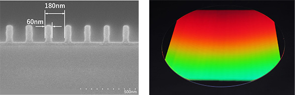
Figure 1: Experimental data
(2) Pitch accuracy of 0.01nm achieved with our unique adaptive optical metrology
Ushio's interference lithography equipment can directly measure interference fringes for exposure with an accuracy of 0.01nm. It also has an adaptive optical metrology to compensate for misalignment with the aiming pitch. This feature makes it possible to achieve the high pitch accuracy required for DFB laser diffraction gratings. (Figure 2)
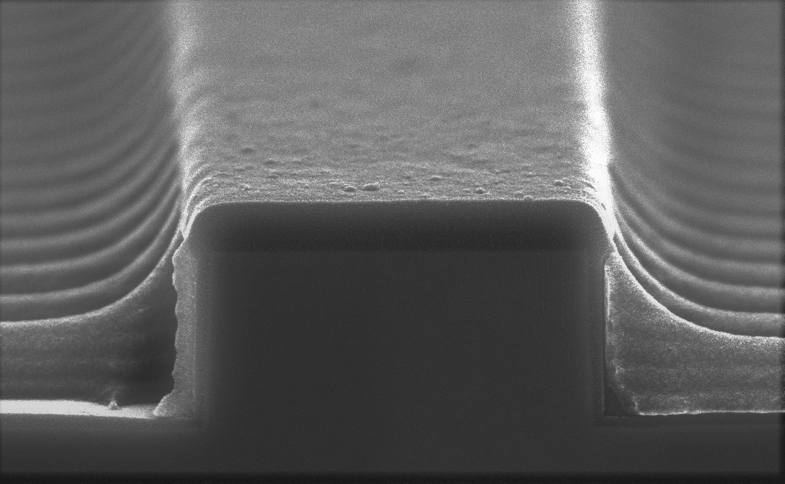
Figure 2: Example of application to DFB laser (SEM image of patterning on a waveguide)
(3) Formation of phase shift structures in combination with digital holographic elements
The phase shift layer is known to improve yield by giving a discontinuous shape to a part of the diffraction grating. Ushio's interference lithography equipment uses a highly controlled digital holographic element to realize a CPM (Corrugation Pitch Modulation) structure with functions equivalent to those of a conventional phase shift layer.
Prior to the product launch, we are widely accepting orders for demonstration processing. This equipment has great applicability not only for Semiconductor Laser Diode (LD), but also for manufacturing optical components needed in AR (Augmented Reality).
Ushio will continue to realize technological innovation in the Industrial Process area with "Light."
The details of this technology will be presented at the IEICE Society Conference (Okayama University) scheduled for September 8th to 12th.
* Technology that integrates electronic circuits handling electrical signals and light circuits handling light signals to replace electricity with light for data processing and communication, aiming for higher speed, lower power consumption, and higher capacity.
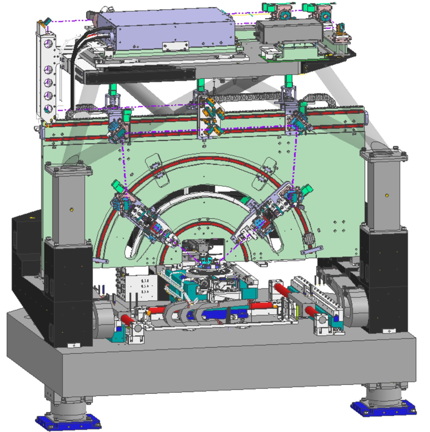
■3D-CAD drawing
■Outline of equipment specifications
| Substrate size | 8 inches or less |
| Substrate thickness | 2mm or less |
| Resolution | 150nm to 650nm |
| Shot size | 13.8 x 13.8mm and 22 x 23mm under development |
| Alignment accuracy | 1μm |
| Transfer type | Cassette-to-cassette transfer |
| Throughput | Approx. 5 wph for 6 inch wafer (depends on exposure method) |
| Footprint | 2.5 × 4m |
| Substrate material | Silicon, glass, compound semiconductors, ceramic materials in general, and other adsorbable materials |
| Exposable patterns | Line-and-space pattern, dot pattern |
| Duty control | Possible by adjusting exposure (0.3 to 0.55), depending on resist type |