USHIO Announces Debut of Two New UX4-LEDs Series Models at SEMICON WEST 2011
Achieving Better CoO by Further Enhancing Productivity and Yield
for High-Volume Manufacturing of HB LED Chips
TOKYO, JAPAN, JULY 11, 2011 — USHIO INC., (Headquarters: Tokyo, Japan; President and Chief Executive Officer: Shiro Sugata, http://www.ushio.co.jp), today announced that the company has started shipping the world’s first 200-mm wafer full-field projection lithography tool “UX4-LEDs FFPL 200” for manufacturing High-Brightness LED chips, and has completed development of the laser lift-off system “UX4-LEDs LLO 150” for volume manufacturing of vertical-structure LED chips.
These latest models of the UX4-LEDs s are based on the same platform as USHIO’s field-proven UX series, which has an installed base of more than 1,100 systems. They will be exhibited through a panel display at SEMICON West 2011, to be held on July 12 through July 14 at Moscone Center in San Francisco, California. (Booth #2633)
UX4-LEDs FFPL 200: a 200-mm Wafer Full-field Projection Lithography Tool
The UX4-LEDs 150-mm wafer full-field projection lithography tool, released last November, has already been used for high-volume manufacturing of LED chips at world-leading LED manufacturers in Japan, Korea, Taiwan, and China, where it has proved its high performance and high reliability. The UX4-LEDs FFPL 200 announced today is mounted with a full-field projection lens of 200 mm in diameter on the common UX4-LEDs platform to enable full-field projection exposure of a 200-mm wafer; it can achieve a high throughput of 120 wafers per hour. Unlike the stepper systems that lower their productivity as the wafer becomes larger, the UX4-LEDs FFPL 200 uses the full-field projection method to enhance its productivity by increasing the wafer size. Therefore, it allows further enhancement of the productivity and reduction of the Cost-of-Ownership (CoO) in the LED lithography process.
Product Features
- Designed to automatically handle wafer size conversions for up to 200-mm wafers
- Completely non-contact so as to cause no mask damage
- Special alignment technology for low visibility alignment marks
- Large depth of focus and special wafer chucking to cope with warped wafers
- Modular platform for future upgrades
- Optional backside alignment function to support LED wafer-level-packaging applications
UX4-LEDs LLO 150: a 150-mm Wafer Laser Lift-off System for HVM of Vertical Structure LED Chips
The laser lift-off (LLO) technology, for stripping a GaN film from a sapphire substrate, is indispensable to increase LED brightness. Leveraging the field-proven photolithography excimer laser, well known for high repetitive frequency and high stability as well as proven DUV optical technologies, USHIO has succeeded in developing the UX4-LEDs LLO 150 laser lift-off system that can achieve both high yield and high throughput. This system also make a contribution to significant reduction of the LED manufacturing cost because it allows reuse of a sapphire substrate by stripping the GaN film from the entire sapphire substrate surface.
Product Features
- Designed to process 150-mm sapphire substrates
- Enable reuse of sapphire substrates, thereby allowing significant reduction of LED manufacturing cost
Common UX4-LEDs Platform
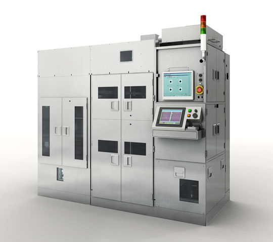
Common UX4-LEDs Platform
Appendix
- UX4-LEDs Product Data Sheet
 (PDF:1.86MB)
warning for UX4-LEDs LLO 150
An act of carrying out the liftoff process using the equipment could infringe the patent rights of Japanese patent No.4285776 and the corresponding patent rights of other countries.
Customers are required to implement the necessary measures at their own responsibility.