USHIO Introduces Three Lithography-System Models
for Power Devices, MEMS, and 3D LSI Devices
USHIO INC., (Headquarters: Tokyo, Japan; President and Chief Executive Officer: Shiro Sugata, http://www.ushio.co.jp/en/) (TOKYO: 6925), today announced that the company is introducing three new models of its "UX4 Series※1" of modular full-field projection lithography tools: the "UX4-ECO FFPL 150" for manufacturing power devices compatible with MPA masks※2 the "UX4-MEMS FFPL 200" with the overlay accuracy of 0.5 µm for manufacturing MEMS devices mounted with the newly developed lens module having a maximum depth of focus of 500 µm and the auto mask changer module for manufacturing multiple device types; and the "UX4-3Di FFPL 300" mounted with a full-field projection lens of 300 mm in diameter for manufacturing 3D LSI devices on 300-mm wafers. USHIO will complete development and start marketing these models one-by-one within the next six months.
These three models will be exhibited and detailed through a panel display as well as a stage presentation at USHIO booth No. 5A-606 (Hall 5) during SEMICON Japan 2011, which will be held December 7 through December 9 at Makuhari Messe in Chiba, Japan.
|
※1 This is the generic name of the lithography systems for semiconductors, FPDs, printed-circuit boards and MEMS devices that USHIO has been manufacturing and marketing for over 20 years. Today, approx. 1,100 UX series units are up and running around the world. The UX series employs all the major lithography methods, including proximity exposure, contact exposure, full-field projection, and step-and-repeat methods, while being capable of handling a wide range of substrates such as wafers, PCBs, and role-to-role flexible substrates. USHIO also develops original light sources and optics including lens and mirrors, mask/substrate transfer components, and other elemental technologies such as alignment technologies. ※2 These are masks used exclusively by the Mirror Projection mask Aligner (MPA) lithography systems manufactured by Canon Inc. Although the manufacture of MPA systems has been discontinued, there are some demands for alternative systems that can use these MPA masks. MPA is a registered trademark of Canon Inc. |
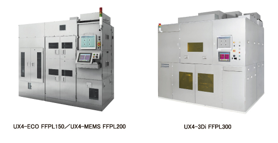
UX4-ECO FFPL 150:
A 150-mm wafer, MPA mask-compatible, full-field projection lithography tool for manufacturing power devices
Using the same platform as the UX4-ECO model for manufacturing power devices, released last November, the UX4-ECO FFPL 150 announced today is mounted with a mask-compatible module that allows use of the MPA masks widely used for manufacturing power devices (in particular, discrete devices).
In addition, for the optics, the newly developed high-performance 150-mm-diameter lens, which is the mainstream for manufacturing power devices, has achieved unparalleled resolution of L/S = 2/2 µm. This allows not only updating of the lithography tool without changing the existing manufacturing process but also further enhancement of the throughput with the full-field projection method. (Available in June 2012.)
Product Features
- Mounted with the newly developed 150-mm full-field projection lens, with unparalleled resolution of L/S = 2/2 µm
- Compatible with MPA masks
UX4-MEMS FFPL 200:
A 200-mm wafer, full-field projection lithography tool for manufacturing MEMS devices
For MEMS devices, the required performance and production volume vary depending on their device types. Therefore, the lithography tool needs to be customized and optimized for each device type.
The UX4-MEMS FFPL 200 announced today, a full-field projection lithography tool dedicated to MEMS manufacturing, allows flexible combination of high-performance modules to meet specific device needs or to upgrade the system itself. These modules include a newly developed lens module with a maximum depth of focus of 500 µm, a 30-stage auto mask changer, and a specially designed wafer transfer module that can handle warped wafers and special substrates.
In addition, the double alignment camera system or DC system enables simultaneous projection of the top and backside of a wafer for high-precision machining from both sides of wafer. (Available in December 2011.)
Product Features
- Top and backside alignment accuracy of 0.5 µm or less
- Large depth of focus of 500 µm or less
- 30-stage auto mask changer to meet the requirements for manufacturing multiple MEMS device types
- Customized chucking plate and transfer module for special substrates
- DC system for simultaneous projection of both sides of wafer (option)
UX4-3Di FFPL 300:
A 300-mm wafer, full-field projection lithography tool for manufacturing 3D LSI devices
As mobile devices such as smart phones evolve, the needs for 3D integration technologies have increased. However, use of TSV (Through Silicon Via), the most promising technology for implementing 3D device structures, has been confronting a big challenge: cost reduction.
We at USHIO have achieved high throughput of 120 300-mm wafers per hour, as well as up to 50% of reduction in CoO by mounting the new 300-mm full-field projection lens on the same platform as the UX4-3Di FFPL 200, released this September. (Available in December 2011.)
Product features
- Designed to mount the 300-mm full-field projection lens
- High throughput of 120 300-mm wafers per hour
- Supports both backside alignment and IR alignment functions
- Allows projection of a thick photoresist film of 50 through 100 µm at a high aspect ratio
- A simple full-field projection method that allows higher uptime
Common products