Accepting Orders for the LED Light Source–Equipped New Products “UX-44101SCB / UX-45114SCB” of the UX-4 Series, Full Field Projection Aligner for Wafers
Ushio Inc. (Head Office: Tokyo; President & CEO: Takabumi Asahi; hereinafter “Ushio”) hereby announces that it will begin accepting orders for “UX-44101SCB” and “UX-45114SCB,” new products equipped with LED light source in the UX-4 Series, full field projection aligner for wafers, starting July 2026.
The UX-4 series is a full field projection aligner that has a proven track record over many years as lithography equipment that enhances production efficiency, primarily for power semiconductors, MEMS sensors, and devices related to the communication and photoelectronic fusion (optical semiconductors.)
In recent years, environmental regulations concerning the use and emission of chemical substances have tightened in the semiconductor industry, impacting the entire sector. Against this backdrop, adoption of LED light sources in lithography equipment has been progressing. However, extending exposure times due to insufficient intensity remains a challenge for layers requiring a high exposure dose.
To address this challenge, based on the solid-state light source design technologies cultivated since its founding, Ushio developed an LED light source unit that achieves intensity equivalent to conventional mercury lamps and has successfully developed the UX-44101SCB and UX-45114SCB, incorporating this LED light source unit.
As next-generation electronic devices essential to the evolution of IoT, 5G, and mobility drive the demand for larger wafer sizes and higher-precision layers, even processes requiring high exposure dose—such as Bump※1 and WLP※2 can achieve high throughput equivalent to conventional mercury lamp equipment. In addition, compared with conventional mercury lamps, the equipment enables instantaneous turn-on and turn-off during exposure, thereby extending the lifetime of the light source and significantly reducing running costs after installation.
As a leading company in full field projection aligner for wafers, Ushio will continue to contribute to the realization of a convenient and comfortable society through light.
※1 A process to form microscopic bump-shaped metal terminals called "bumps" (such as solder balls) on the electrode parts of semiconductor chips.
※2 A process to perform batch packaging (encapsulation) and terminal formation on the whole wafer before cutting the silicon wafer into square chips.
■Main Features
・Full field projection exposure: No Mask damage, High productivity 120 WPH or more
・Deep depth of focus: Exposure to 3D surface shapes, Thick film resist exposure
・Automation compatible: Inline, Online, OHT/AGV
・Mercury-free: Compatible with LED light sources
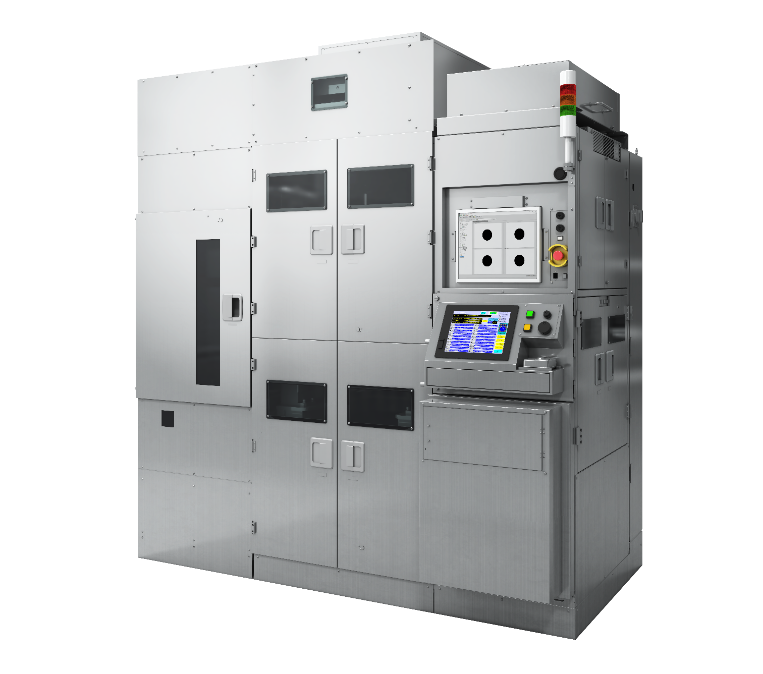
■Appearance
■Specification
| Specifications/Model | UX-44101SCB | UX-45114SCB (Provisional specifications) |
UX-45114SC (Lamp Light Source) |
| Wafer size | 4inch | 6inch/8inch | 6inch/8inch |
| Exposure field size | φ100mm | φ200mm | φ200mm |
| Resolution | 2μm | 2.8μm | 2.8μm |
| Depth of focus | ±10μm | ±10μm | ±10μm |
| Overlay accuracy (Top side) |
±1.0μm | ±0.8μm | ±0.8μm |
| Overlay accuracy (Back side) |
±1.5μm | ±1.0μm | ±1.0μm |
| Wavelength | i Line | i Line | i Line |
| Intensity | 100mW/cm2 | 40mW/cm2 | 40mW/cm2 |
| Supported wafer materials |
Si, GaAs, GaN, GaP, InP, SiC, |
||
| Automation Options | EFEM, Automatic mask handling, SECS/GEM online, AGV, Inline with coater/developer |
||
