光技術情報誌「ライトエッジ」No.22(2001年9月発行)
IPC Printed Circuits Expo 2001技術フォーラム
Presented at IPC Printed Circuits EXPO® 2001
www.ipcprintedcircuitexpo.org
(2001年4月)
The Latest Alignment Technology in PCB Step-and-Repeat
Projection Exposure System
Yoneta Tanaka, Ryozo Matsuda, Kazuki Shinoyama, Jun Homma
USHIO, Inc.
Yokohama, Japan
General
There are three typical challenges in manufacturing PCBs: enhancement of the overlay accuracy of the exposure pattern, decrease in the fine pattern size, and enhancement of the product yield. To meet these challenges, the step-andrepeat projection exposure method using a projection lens is effective. As its most prominent feature, the step-andrepeat projection exposure method allows non-contact patterning. It can also measure the expansion/contraction ratio of the actual pattern at each shot so as to allow projection of the mask at the corresponding expansion/contraction ratio.
It can be considered as essential in the future to introduce this system into production of the interposer boards for BGAs/CSPs, which are expected to increase in its production volume, and the PCB for digital equipment.
This paper presents basic studies of the step-&-repeat projection exposure system, especially its alignment technology.
Introduction
In recent years, high resolution and high overlay accuracy have been required for PCB such as MPU packages. We at our company developed The Step-&-Repeat Projection Exposure System for PCBs aiming at the achievement of high resolution, high overlay accuracy and enhancement of the product yield.
The standard at which the step-and-repeat projection exposure method becomes effective is for products that require an overlay accuracy of within ±30 µm and a minimum line width of within 50 µm. In addition, this method is effective for cases in which a mask defect has caused a series of workpiece defects. A PCB expands or contracts asymmetrically during production. The conventional systems, contact/proximity-type-exposure systems, for example, have reduced deterioration in the overlay accuracy by correcting the mask. However, because the expansion/contraction amount varies in different areas within the same board, the conventional system has a limit in enhancement of the overlay accuracy and yield. It can therefore be considered that the use of the step-and-repeat projection exposure method and auto scale function is essential for exposure of PCBs at high accuracy.
In addition, the projection exposure system generally uses an off-axis alignment method, which has difficulty in implementing closed-loop alignment. We have solved this problem by utilizing on-axis TTL alignment using a non-exposure wavelength.
We consider that application of the step-and-repeat projection exposure system to future manufacturing of PCBs as the most important challenge.
Alignment Method
On-Axis TTL Alignment with Non-Exposure Wavelength
As the alignment method, the step-and-repeat exposure system utilizes on-axis TTL alignment using a non-exposure wavelength. The projection lens is usually designed to obtain the required resolution with the exposure light (to correct the aberration). For this reason, off-axis alignment is generally used to partially radiate the exposure wavelength as an alignment light. Use of the exposure wavelength for alignment causes the area surrounding the alignment mark to be exposed during alignment. If the required resolution is low, it can be considered to use the projection lens that corrects the aberration with two lines: the exposure wavelength and the non-exposure wavelength (generally 546 nm). However, as the required resolution becomes higher and the exposure area becomes larger, this method may not be used.
On-axis TTL alignment using a non-exposure wavelength is effective to solve this problem. The method works as follows:
Figure 1 shows the method for calibrating the relative positions of the mask and the vision of the alignment microscope. The mask image can be directly observed by the exposure wavelength. Under this condition, there is only the mask alignment mark in the vision of the detection system. Therefore, it is not necessary to consider interference with the workpiece alignment mark.
First, the exposure light is radiated around the mask alignment mark image on the workpiece-stage mirror. The image formed by the mirror is detected by the alignment microscope, and the image position is saved in memory. At this time, the exposure light is radiated onto the mirror section only. Therefore, the substrate is not exposed. Saving the image position, the system quits radiating the exposure light, and the workpiece stage moves to the position for detecting the alignment marks on the substrate.
Figure 2 shows the method for detecting the workpiece alignment mark. As the light used to illuminate the workpiece alignment mark, a nonexposure wavelength light is introduced from the alignment microscope via an optical fiber. This allows independent detection of the workpiece alignment mark regardless of the mask alignment mark. After detection of the workpiece alignment mark, the workpiece is moved for alignment. The relative positions of the mask and the alignment microscope do not change within a short period of time. Therefore, the on-axis TTL allows alignment with the non-exposure wavelength. This is the alignment method proposed by us.
This allows perfect matching of the mask alignment mark and workpiece alignment mark and completes the alignment process. The alignment optical system is retracted from the workpiece stage and the system starts the exposure process.
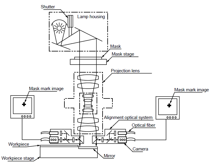
Figure 1 - Alignment Process of Detecting the Mask Alignment Mark
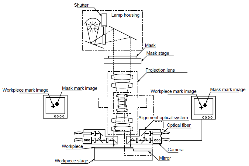
Figure 2 - Alignment Process of Detecting the Alignment Marks on the Substrate
Three Alignment Modes
The system throughput and the overlay accuracy vary depending on the alignment mode selected during the exposure process. It allows any of the following three alignment modes to be selected.
(1) Die-by-die
This allows direct alignment of the mask alignment mark and workpiece alignment mark for each exposure run. Therefore, the alignment performance is expected to be completed as a closed loop.
(2) Quasi die-by-die
This allows direct alignment of the mask alignment mark and workpiece alignment mark for an exposure of the first shot of each workpiece. In this case, the exposure process is performed on assumption that the relative positions of the mask and alignment microscope do not change.
Since the die-by-die alignment requires alignment process of detecting the mask alignment mark for each shot, the total throughput is lowered. On the other hand, when quasi die-by-die alignment is used, the total throughput is higher.
(3) Global
The conventional step-and-repeat exposure systems, semiconductor steppers and LCD steppers, for example, use this method. This mode estimates the designed exposure position from the reference marks on the workpiece and performs exposure of each shot. In the production of PCBs, Global is not so practical because they have expansion or contraction asymmetrically during production, whose amount varies in different areas within the same board.
Among the above three alignment modes, the quasi die-by-die mode is the most practical alignment mode. The throughput of the system operating in this mode can be calculated by the following formula:
Process time per layer = (Alignment time + Exposure time) x Number of shots + Time required for workpiece replacement
Where the alignment time and the time required for workpiece replacement are approximately 1.5 seconds and 10 seconds, respectively.
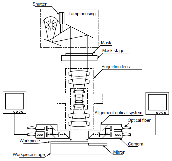
Figure 3 - Exposure Process
Auto Scale Function
On the PCB, expansion/contraction of the pattern varies greatly depending on the process. From experience, the maximum expansion/contraction amount ranges from 250 ppm to 500 ppm. Variance of the expansion/contraction amount may reach approximately. 100 ppm within the same lot. The actual expansion/contraction amount of the board varies depending on the individual board characteristics. Thus, it is difficult for the mask correction method to achieve a high overlay accuracy.
The auto scale function of this system allows expansion or contraction of the mask image projected on a workpiece by changing the projection magnification. The projection magnification is determined by measuring the actual pitch of the workpiece alignment mark.
Effectiveness During Processing of Actual Boards
Expansion/Contraction of PCBs
The expansion/contraction of an actual PCB varies depending on the base material, machined patterns, process conditions and other factors (see Figure 4). The system allows measurement of the expansion/contraction amount of the actual board during exposure process. Either two or four measuring points can be selected at determination of the system specifications. For a normal PCB, the expansion/contraction amount differs between the horizontal (X) and vertical (Y) directions. Therefore, it is desirable that the projection magnification is determined by measuring the expansion/contraction amount in both the horizontal and vertical directions.
On the sample measured by us, variance in the pitch was ±4µm (3 σ : 5.5µm). Also, it can be proved that the expansion/contraction amount differs between boards and shots within a board and that there is no systematic trend.
The size of the boards generally used ranges from 510 mm x 340 mm to 340 mm x 255 mm. Based on the proceeding data, variance in the pitch may reach ±20µm for 500 mm. This is the data obtained during processing of samples; variance in the expansion/contraction amount during processing of an actual workpiece may become further greater.
From such behavior, as shown in the proceeding, during expansion/contraction, it becomes impossible to handle expansion/contraction of the board with the conventional mask correction method. For example, if an overlay accuracy of ±25µm is required, it can be considered to deteriorate the product yield.
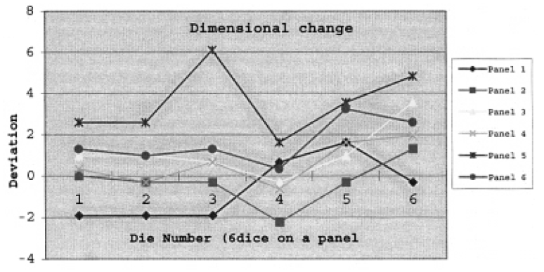
Figure 4 - Marks on the Substrate
Advantage of Auto Scale Function During Overlay Exposure
The following shows a pattern shift measured at the alignment mark after exposure of a sample board. The sample board is 510 mm x 340 mm, and six shots of exposure are performed at two rows by three columns. As the process recipe for exposure, the alignment tolerance is ±1 µm in the X/Y direction and the pitch tolerance is ±1 µm. The pitch tolerance is used to correct the mask size with the auto scale function.
Evaluation performed has proved that the overlay accuracy of approximately ±5 µm can be achieved by optimizing the exposure area. The evaluation result is introduced as follows:
Number of samples: 90 shots
Measuring instrument: Mitsutoyo Quick Vision (QV606 Super)
Measurement repeatability: ±1 µm
The variances at the alignment mark estimated from the log data obtained during the exposure process were 2.3 through 2.6µm (3 σ ) (see Figure 5). The measurement results of the actual workpieces include variance of the measurement repeatability and varianace of each alignment mark. Therefore, it can be considered that these results are greater than th variances estimated from the log data.
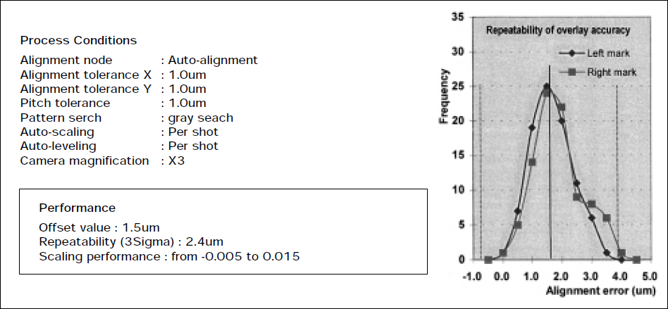
Figure 5-Process Conditions
The Latest Technology of Detecting Alignment
In order to achieve a high overlay accuracy, auto scale function is very effective, however, there are other critical problems in the alignment process. Those are unstable shape, contrast and appearance of alignment marks on the substrate, which make the alignment performance deteriorated. The alignment mark detection method of the step-and-repeat exposure system is pattern matching with gray image processing. The recognition condition of the alignment marks varies depending on the photoresist, under-layer, etc. Therefore, the alignment accuracy is greatly affected by the recognition condition.
We have developed the center detection method to avoid the influence of an unstable appearance of alignment marks. The interim report is as follows.
Estimation method: The repeatability of detecting positions of alignment marks
N: 50
Repeatability (3sigma): (see Figure 6 and Figure 7)
Center detecting method X:0.61 Y:0.79
Conventional pattern matching X:3.19 Y:4.14
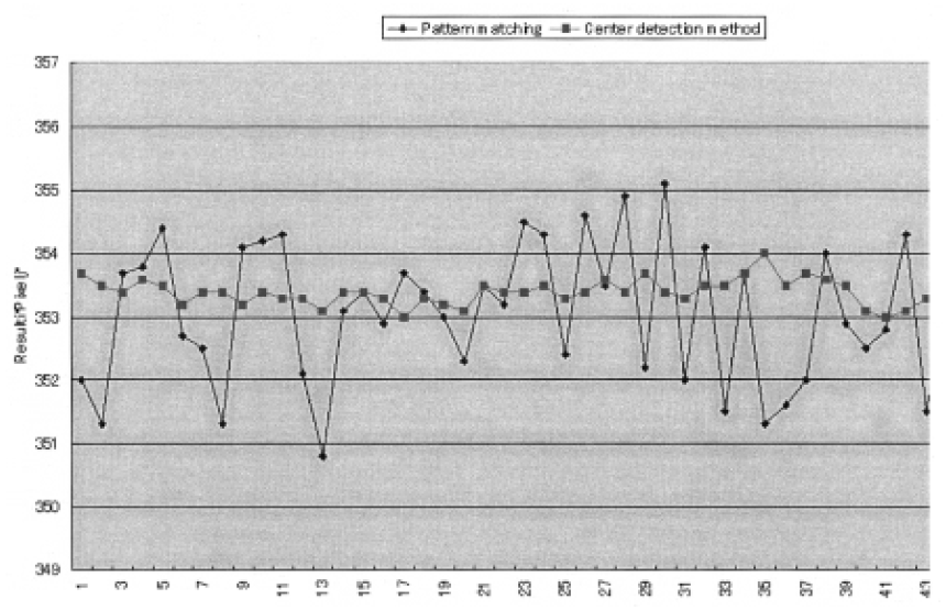
Figure 6-Detection Position of X
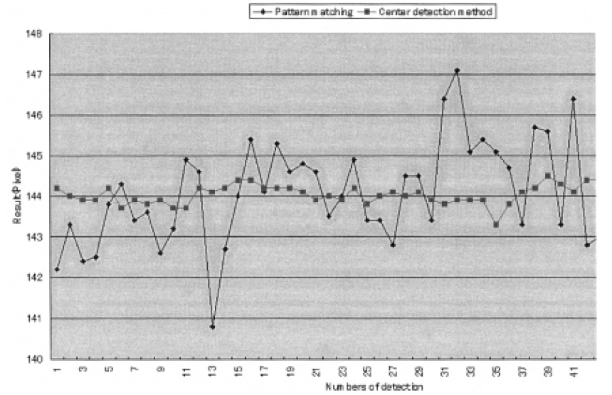
Figure 7-Detected Position of Y
Summary
Step-and-repeat projection exposure systems for PCBs have been on the market at least since April 1999. The systems feature an exposure process with no contact between a substrate and the mask, high alignment accuracy achieved by utilizing TTL on-axis alignment using a non-exposure wavelength and provision of the auto scale function.
Enhancement of the overlay accuracy and non-contact exposure process allows achievement of a high yield and margin of the process other than exposure. It can be expected that the demand for the boards mounted with flip-chip devices will increase. In such a technological trend, the step-and-repeat projection exposure technology will become indispensable.
