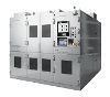
Development of panel-level organic lithography equipment for advanced packaging
Naoya Sohara,Yu Abe, Sho Yamauchi, Ryotaro Takahashi, Hirosuke Takamatsu
Ushio Inc. 1-90 Komakado,Gotenba city, Shizuoka pref, Japan
In recent years, “heterogeneous integration” has become popular in semiconductors, where multiple chips are connected on a single substrate to achieve high performance and high functionality. With the development of this technology, conventional lithography equipment for organic substrates are required to achieve both miniaturization and large area exposure. This paper summarizes recent issues in lithography equipment for organic substrates.
First, this paper compares the lithography process in the semiconductor front-end process with that in the back-end process. Then, it shares the back-end-specific lithography equipment challenges caused by the SAP process commonly used in the back-end process. Finally, he showed that for back-end lithography equipment, it is important to have both DOF and resolution with appropriate NA and a system that can achieve multi-point alignment at high throughput to deal with distorted substrates.
For papers (You are leaving for an external site.)
Copyright © USHIO INC. All Rights Reserved.