光技術情報誌「ライトエッジ」No.31
2007.11 Fifth international symposium on control of semiconductor interfaces
(2008年10月)
Role of UV Irradiation during Si Etching Process in Chlorine Plasma
Butsurin Jinnai,1 Fumihiko Oda,2 Yukihiro Morimoto,2 and Seiji Samukawa1
1 Institute of Fluid Science, Tohoku University, 2-1-1 Katahira, Aoba-ku, Sendai 980-8577, Japan
TEL/FAX: +81-22-217-5240 ; E-mail : samukawa@ifs.tohoku.ac.jp
2 R&D Center, Ushio Inc., 1194 Sazuchi, Bessho-cho, Himeji, Hyogo 671-0224, Japan
1. Introduction
For the past 30 years, plasma processes have been used to shrink the pattern size of ultra-large-scale integrated (ULSI) devices. High-density plasma sources, such as inductivelycoupled plasma (ICP) and electron-cyclotronresonance plasma, are particularly important for developing precise etching processes. However, in future nanometer-scale ULSI devices, the chemical reactions on the surface atomic layer must be accurately controlled to enable precise patterning without causing irradiation damage during plasma etching. Especially, the effects of photon irradiation from plasma to surface must be understood in order to control the atomic layer reaction and suppress the generation of defects on the surface during the plasma etching process.
In this study, we investigated the effects of photon irradiation during high-density Cl neutral beam etching[1-3] of Si by combining a UV lamp. In this process, Si can be etched with controlling photons (wavelength and intensity) in the similar situation to plasma processes. Our goal was to understand the effects of wavelength and density of irradiated photons on surface reaction and the role of UV photon irradiation from the plasma on etching reactions during the chlorine plasma Si etching processes.
2. Experimental
Our neutral-beam (NB) source consists of a process chamber and parallel carbon electrodes (top electrode and aperture), as shown in Fig. 1. The chamber is separated from the process chamber by a carbon plate (aperture) that is fitted at the bottom. Numerous apertures in the bottom of the carbon plate enable neutral beams from the plasma to pass into the process chamber. The accelerated ions in the plasma are effectively neutralized by a charge transfer when they pass through the apertures. In addition, the photons generated in the plasma chamber are almost entirely eliminated while passing through the apertures because the UV light from the plasma is effectively absorbed and/or shaded in the apertures of the carbon plate. Application of an RF bias of 600 kHz to the bottom of the carbon plate enables a low-energy, collimated neutral beam ranging from 10 to 100 eV to be generated with a high-density flux of about 1 mA/cm2. Apart from the effect of photon irradiation, the beam and radical flux were almost the same as those in conventional Cl plasma etching conditions.
The UV lamp was set at 90° to the neutral beam source. We used a short-arc Xe flash lamp (pulse discharge) for irradiating UV photons to the Si sample surface. The irradiated light had a spectrum from 200 nm to the visible region. We observed higher photon intensity in the UV region from 220 to 400 nm than in the visible region. We monitored the power density of the irradiated photons using a calory meter, and the total power density was controlled in the range of 0 to 50 mW/cm2 . The photon irradiation frequency was fixed at 8 Hz [pulse width of on-time was 25 µs in full-width at half maximum]. Furthermore, we were able to cut the UV photons with wavelengths of less than 380 nm using the UV photon filter and determine the effects of UV photons and visible photons onthe surface reactions.
The substrate was 220 mm from the apertures, and the angle of the substrate surface was fixed at 45° to the direction of the neutral beam irradiation and photon irradiation. The Si etching depth was measured using atomic force microscopy.
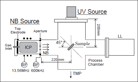
Fig.1: Our developed neutral beam source and UV lamp.
3. Results and Discussion
We investigated the effects of photon irradiation (total power density : 38mW/cm2 , frequency: 8 Hz)on etching depth as a function of RF bias power. We used two types of irradiated photon wavelengths : more than 200 nm and more than 380 nm. Changing the RF bias power from 0 to 80 W enabled the Cl beam energy to be controlled from 10 to 100 eV. As shown in Fig. 2, irradiation of UV photons (from 200 to 380 nm) dramatically increased the etching depth under all RF bias conditions; however, irradiation of visible photons did not increase the etching depth at the same power density. These results suggest that UV photon irradiation effectively enhances the surface chemical reaction when Si is etched with a chlorine atom beam.
Figure 3 shows the dependence of the etching depth on the photon irradiation power density (wavelengths from 200 to 380 nm) in the same neutral beam conditions (same beam energy and flux). The RF bias power for controlling the neutral beam energy was fixed at 60 W (etching time: 20 min). The Si etching depth increased dramatically with the photon irradiation power when the power (wavelengths from 200 to 380 nm) was greater than 6 mW/cm2. We first found that a photon irradiation power density over 6 mW/cm2 was particularly effective in enhancing surface reactions between Cl and Si.
These results show that UV irradiation from 200 to 380 nm enhances the surface reactions and that the effects of UV irradiation strongly depend on UV-irradiation power density. We speculate that UV-irradiation generated defects on the Si surface and the Cl etching reaction was effectively enhanced within the defect region on the Si surface during chlorine plasma etching.
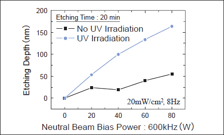
Fig.2: Effects of photon irradiation(total power density:38mW/cm2, frequency: 8Hz) on etching depth as a function of RF bias power during Cl neutral beam etching. Irradiated photon wavelength was changed using UV photon filter.
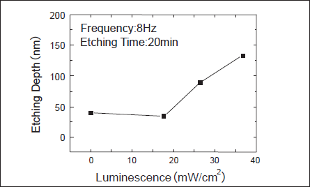
Fig.3: Dependence of etching depth on photon irradiation power (wavelengths from 200 to 380 nm) in same neutral beam conditions (beam energy and flux).
4. Conclusion
We found that UV from 200 to 380 nm dramatically enhances Cl reactions with Si when UV power of over 6 mW/cm2 is irradiated during chlorine neutral beam process. We also controlled the Si etching rate by changing the UV-irradiation power. Experimental results suggest that the UV photon irradiation to the surface dramatically enhances surface reactions during chlorine plasma etching. We believe this is due to the generation of crystal defects by UV irradiation on the Si surface.
関連製品
論文を探す
デジタルサイネージへの応用が期待されているバックライトや、医療分野で注目されている光線力学療法など、2007年春から2008年夏にかけて発表した論文を中心に掲載しています。
(2008年10月)