光技術情報誌「ライトエッジ」No.33(2010年8月発行)
2010.1 Applied Physics Letter
Stress-Enhancement in free-standing Si pillars through
nonequilibrium dehydrogenation in SiN:H
stress-liners by ultraviolet light irradiation
Takanori Tanaka,1 Taizoh Sadoh,1,a) Masashi Kurosawa,1 Masanori Tanaka,1
Masanori Yamaguchi,2 Shinji Suzuki,3 Tokuhide Kitamura,4 and Masanobu Miyao1
1Department of Electronics, Kyushu University, 744 Motooka, Fukuoka 819-0395, Japan
2USHIO INC., 1194, Sazuchi, Bessho-cho, Himeji 671-0224, Japan
3USHIO INC., 2-6-1 Ohtemachi, Tokyo 100-8150, Japan
4Toshiba Semiconductor, 1-10-1 Shimoitozu, Kitakyushu 803-8686, Japan
(Received 10 October 2009; accepted 7 December 2009; published online 28 December 2009)
Tensile-strained Si pillars are desired to achieve three-dimensional (3D) transistors with high speed. Effects of ultraviolet (UV) light irradiation on tensile strains in Si pillars covered with SiN:H stress-liners are investigated as a function of the wavelength (172‒436nm) . Tensile-stress enhancement is found at specific wavelengths (200‒330nm) under low-temperature heating (400°C), where dehydrogenation in SiN:H is clearly detected by infrared absorption measurements. On the other hand, equilibrium dehydrogenation by high-temperature heating (>700°C) without UV-irradiation does not cause tensile-stress enhancement. This nonequilibrium dehydrogenation at low temperatures opens up possibility of 3D transistors with high carrier mobility.
©2009 American Institute of Physics [doi:10.1063/1.3278596]
Strained Si-on-insulator (SOI) is promising for break-through the scaling limit of complementary metal-oxide-semiconductor transistors (CMOS), because of the mobility enhancement together with the reduction in parasitic capacitance and leakage current.1-3 Thus, various techniques to obtain strained SOI are investigated. These techniques can be classified into two types, i.e., the global and local techniques. In the global technique, Si layers are epitaxially grown on SiGe buffer layers on insulator.4-7 However, this is not applicable to three-dimensional (3D) structures, such as vertical-channel transistors, which will be utilized in the next-generation CMOS. Thus, development of the local technique using stress-liners, such as SiN:H, is necessary.
To obtain a sufficient mobility enhancement, large tensile-strains (~1%) should be induced in Si. Tensile strains are induced by SiN:H liners formed by plasma-enhanced (PE) chemical vapor deposition (CVD) at low temperatures. The strains can be increased to 0.3%‒0.4% by increasing H concentrations.8,9 Recently, enhancement of tensile strains (~1.3%) by ultraviolet (UV) irradiation, with a broad wavelength (>200nm), during annealing (~400°C) of SiN:H liners has been demonstrated.10,11 However, it was reported that H concentrations decreased by irradiation, which apparently contradicted to the previous reports.8,9 Moreover, the wavelength range, effective to enhance strains, was not clarified. Effects of the H concentration and the wavelength should be clarified to establish the physical mechanism for optimization of the UV irradiation conditions.
Recently, Wang et al.12 investigated strain-introduction in SiN-deposited Si cantilevers , obtained by patterning of top Si and removal of underlying buried oxide (BOX) of SOI wafers, by photoluminescence measurements. This demonstrates that the Si cantilevers are useful for simulation to examine the strain-introduction in free standing Si pillars for the vertical-channel structures.
In the present study, effects of UV irradiation on strains in SiN:H-deposited Si cantilevers are investigated, and the wavelength effective for strain enhancement is clarified. Moreover, the mechanism of strain enhancement is discussed on the basis of the change in H concentrations in SiN:H.
In the experiment, SOI wafers (top Si: 340 nm, BOX:2μm) were employed. The top Si was patterned by dry etching. Subsequently, BOX under the patterned top Si was undercut by wet etching. Thus, Si cantilevers (width:3μm, length:20μm) with supporting bases (100x100μm2 ) were fabricated. They were covered with SiN:H (thickness:~150nm) using PE-CVD at 400°C. The sample structure is shown in Fig. 1(a). The samples were annealed at 300‒1050°C for 30 min in N2 without irradiation or at 400°C for 60 min in a vacuum with irradiation (wavelength : 172‒436nm, photon dose rate: 5x10¹⁵‒4x1016cm-2s-1).
The strains in the Si cantilevers, as indicated by the broken circle in Fig. 1(a), were evaluated by microprobe Raman spectroscopy (laser spot: ~1μm Φ, wavelength: 532 nm). The strains (ε) in Si were evaluated from the shift of the Raman peak due to the Si‒Si vibration mode (ΔωSi‒Si) using ε=ΔωSi‒Si/715x100(%).13
Raman spectra for the samples with and without SiN:H are shown in Fig. 1(b). The spectra for the samples without SiN:H have a single peak at 520cm-1,which is due to strain-free c-Si.13 On the other hand, the spectra for the SiN:H-deposited sample consist of two peaks at 516.7 and 520cm-1 . The peak at 516.7cm-1 is due to the tensile strained Si cantilever, while that at 520cm-1 is due to the Si substrate. The change in the peak positions (3.3cm-1) indicates introduction of 0.46% tensile strain.
Since H concentrations in SiN:H can be decreased by annealing without UV irradiation,14 we examined effects of the H concentration on strains by annealing. The infrared (IR) measurements were performed for samples annealed at 300‒1050°C in N2 without irradiation. Typical IR spectra of samples before and after annealing are shown in Fig. 2(a), where the spectra are subtracted with those of the sample completely dehydrogenated by high temperature annealing (1050 °C). Absorption peaks are observed at ~3350cm-1 which are due to the N‒H bonding in SiN:H.15 The peak height decreases with increasing annealing temperature. The concentrations N of N‒H bonds were evaluated using the following equation:15
where K is the absorption coefficient for N‒H bonds (5.3x10⁻¹⁸cm), and t is the film thickness in nanometers. The results are summarized in Fig. 2(b). The H concentration is 2.7x10²² before annealing and scarcely changes after annealing at 400°C. However, it significantly decreases with increasing temperature above 400°C. The Raman measurement of the sample annealed at 600°C indicated that the sample kept a tensile strain (0.31%) . However, the strains changed to compressive after annealing at temperatures above 700°C and became 0.37% (800°C) and 0.43% (1000°C).
The bonding structures in PECVD SiN:H are in non-equilibrium due to low deposition temperatures and high H concentrations, and thus, tensile strains are induced in Si.16 On the other hand, compressive st ra ins a re induced in Si by depositing therma lly relaxed SiN layers by low-pressure CVD(LP-CVD),17 because the intrinsic SiN has shrunk bonding structures.18,19 Thus, it can be concluded that enhancement of tensile strains cannot be realized by dehydrogenation with structural relaxation of SiN:H by high temperature annealing (>700°C). Therefore, a low temperature (<700°C) processing is necessary to enhance the tensile strains.
To examine effects of UV irradiation at low temperatures on tensile strain enhancement in Si covered with SiN:H, strains in the samples after irradiation with three typical wavelengths (172, 308, and 436nm) at 400°C for 60min were evaluated by Raman measurements. The measurements did not reveal Si nanoparticle formation in SiN:H by the irradiation. The strains are summarized as a function of the photon dose rate in Fig. 3. After irradiation with the wavelength (308nm), the strain linearly increases with increasing photon dose rate. On the other hand, irradiation with the wavelengths (172 and 436nm) does not cause any significant change in strains. These results show that irradiation with a specific wavelength, e.g., 308nm, is necessary for strain enhancement. The results clearly indicate the existence of the minimum and the maximum wavelengths for the strain enhancement, which should be key parameters to reveal the mechanism of the enhancement.
To clarify the wavelength dependent strain enhancement, samples were irradiated (photon dose rate: 2x1016cm-2s-1) with various wavelengths (172‒436nm) at 400°C for 60 min. The wavelength dependences of the tensile strains in Si and the N‒H bond concentrations in SiN:H annihilated after irradiation are summarized in Figs. 4(a) and 4(b), respectively. The strains in samples before and after annealing (400°C, 60min) without irradiation are also shown by the broken and dotted lines, respectively, in Fig. 4(a). The tensile strain increases from 0.46% to 0.57% by irradiation with the wavelength (200‒330nm). On the other hand, the wavelengths shorter than 172nm and longer than 365nm are scarcely effective for enhancement. Moreover, the wavelength dependence of the annihilated N‒H concentrations shows a good agreement with that of the strain enhancement, namely, the annihilated N‒H bond concentrations are large(~1.5x1022cm-3) for the wavelength (200‒330nm). The annihilated N‒H concentrations (~15x1022cm-3). is as large as that achieved by heating at 700°C without irradiation, where structural relaxation causes compressive strains, as shown in Fig. 2(b). However, in the irradiated samples, the relaxation does not occur because of the low processing temperature (400°C). Thus, this result clearly demonstrates the importance of H removal without structural relaxation to enhance the tensile strains.
Let us discuss the wavelength effects. Since the band gap energy of SiN is ~5.4 eV,20 the penetration depth of photons into SiN significantly decreases with decreasing wavelength for the wavelength <~200nm, i.e., from penetration depth of 110(wavelength:200)nm to 20nm (wavelength:172nm),20 and thus the irradiation effects are scarcely observed for wavelengths (<200nm).
On the other hand, the maximum wavelength (330nm) for enhancement can be explained as follows. The Si‒N network structures are slightly shrunk before UV irradiation, because distances between N and H atoms become short due to the attractive force induced by the hydrogen bond. The maximum wavelength (330nm), i.e., photon energy (3.8eV), is almost equal to the bonding energy of H atoms with Si or N atoms[Si‒H:3.9eV(Ref.21) and N‒H: 4.1eV (Ref.20)]. Thus, irradiation with higher photon energy (>~3.8eV) can break these bonds, and the Si‒N network structures are expanded with keeping the nonequilibrium bonding structures by removing H, which results in the strain enhancement. These phenomena determine the minimum and maximum wavelengths effective for the strain enhancement. It can be concluded that nonequilibrium dehydrogenation of SiN:H, i.e., dehydrogenation at low temperatures without inducing structural relaxation, is necessary to enhance the strains. The enhanced tensile strain (0.57%) obtained in this study is smaller than the reported value (1.3%).10,11 As suggested from Fig. 3, the strain can be increased by increasing photon dose rate.
In summary, UV irradiation effects on strain enhancement in SiN:H-deposited Si have been investigated. Irradiation (wavelength: 200‒330nm) at a low temperature (400°C) is effective to enhance the tensile strains, due to the nonequilibrium dehydrogenation. This technique is useful to enhance the mobility of 3D transistors for next-generation CMOS.
We are very grateful to Professor H. Nakashima and Dr. Dong Wang of Kyushu University for valuable discussion. This work was supported by a grant of Knowledge Cluster Initiative implemented by Ministry of Education, Culture, Sports, Science and Technology of Japan.
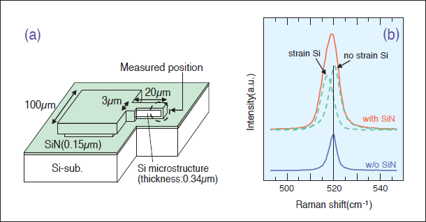
FIG .1: Schematic structure (a) and Raman spectra of Si cantilever with and without SiN:H (b). Raman measurements were performed in the region shown by the broken circle in (a).
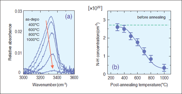
FIG. 2 : Fourier transform IR spectra of sample before and after annealing at 400‒1000°C without UV irradiation (a) and annealing temperature dependence of N‒H bond concentration (b).
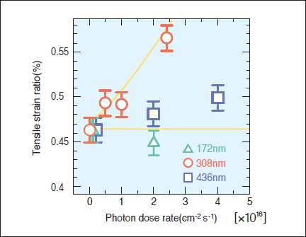
FIG. 3 : Tensile strain in SiN:H deposited Si as a function of photon dose rate of UV irradiation (wavelength: 172, 308, and 436nm, temperature: 400°C, and period: 60min).
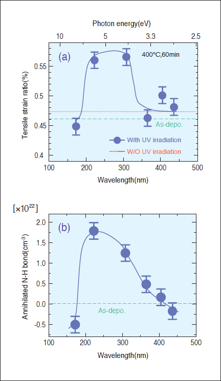
FIG. 4 : Change in tensile strain (a) and annihilated N‒H bond concentration (b) by UV irradiation (photon dose rate: 2x1016cm2s1, temperature: 400°C, and period: 60 min) as a function of wavelength. Data of samples before irradiation are shown by the broken lines in (a) and (b),and those after annealing (400°C, 60min) without irradiation are shown by the dotted line in (a).
論文を探す
FPCの微細化・高生産性を達成する露光装置をはじめ、CSPの高密度化に対応した有機フリップチップパッケージ向け露光装置、精密ドライ洗浄分野で高シェアを占めるエキシマランプ、医療分野で注目を集める免疫分析装置、長年にわたり定評のある太陽電池特性評価用ソーラーシミュレータなど、2009年夏から2010年春にかけて発表した論文10を掲載しています。
また、シリーズ「大学研究室を訪ねて」では、マイクロ・ナノ加工、バイオ・流体デバイスの研究開発に精力的に取り組む、香川大学准教授の鈴木孝明先生の研究室をご紹介しています。
(2010年08月)