光技術情報誌「ライトエッジ」No.39(2013年6月発行)
JJAP
(2013年5月)
Self-Separation of Sublimation-Grown
AlN with AlSiN Buffer Layer
Katsushi Nishino,1,* Jun Nakauchi,1 Kotaro Hayashi1, and Masashi Tsukihara2
1The University of Tokushima, Tokushima 770-8506, Japan
2Ushio Inc., Himeji, Hyogo 671-0224, Japan
*E-mail:nishino@ee.tokushima-u.ac.jp
AlN was grown by a sublimation method on 6H-SiC. We found the grown AlN layer is easily separated from the substrate when Si powder is added to the AlN source powder. The formation of AlSiN layer with the Si content of 15% at the AlN/6H-SiC interface was confirmed by energy-dispersive X-ray spectroscopy and X-ray diffraction. This AlSiN layer causes the separation of AlN.
AlN is one of the candidates for a substrate of nitride-based UV light-emitting diodes (LEDs) because of its wide bandgap of 6.2 eV (UV transparency) and lattice and thermal expansion matching to AlGaN layers used in UV-LED structures. Many research groups are trying to obtain AlN bulk crystal by a sublimation method as reported in, for example, refs. 1-6. Large bulk AlN can be obtained and the characteristics of AlN are widely investigated. However, it needs long time and many processes, such as long-time growth, slicing, polishing and so on, to obtain free-standing AlN which can be used as a substrate.
In this paper, we propose a new method to obtain a free-standing AlN crystal in short time and low cost by introducing an AlSiN buffer layer between the 6H-SiC substrate and the AlN grown layer during the growth by a sublimation method.
Crystal growth of AlN was carried out by a conventional sublimation method. We used a graphite crucible with tungsten cover to reduce carbon incorporation into the grown layer. 6H-SiC (Si-face) was used as a substrate and AlN powder as a source. Si powder was added to the source by (1) mixing with AlN powder (sample 1) or (2) placing on the top of the source (sample 2). The amount of the added Si was less than 0.5 wt%. The temperature of the lid of the crucible during the growth was 1860°C monitored by a pyrometer. The actual temperature in the crucible may be a few hundred degree higher than the lid. The growth pressure was atmospheric in N2 and the typical growth time was 1 h.
The grown layer was observed by a scanning electron microscope (SEM) and examined by X-ray diffraction (XRD) and energy-dispersive X-ray spectroscopy (EDS).
Figure 1 (a) shows a surface SEM image of sample 1 (Si mixed with the source) and (b) of sample 2 (Si placed on the top of the source). Both surfaces are relatively smooth with some hexagonal hillocks. Most of the grown layers are easily separated from the substrates by a light mechanical shock, especially for sample 2. The thickness of the AlN layer is about 30 μm for sample 1 and about 70 μm for sample 2.
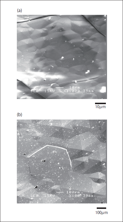
Fig. 1 SEM images of the surface of AlN grown layers. Si was added by (a) mixing with AlN source and (b) placing on the top of AlN sour
The XRD pattern of the sample 2 is shown in Fig. 2. A peak of AlN (0002) is clearly observed and the growth of AlN was confirmed. The full width at half maximum (FWHM) of the peak is 129.6 arcsec and relatively high quality AlN crystal was obtained. In addition to the AlN peak, a broad peak is observed at 36.5° , which may be attributed to AlSiN with the Si content of 15%.7,8) The XRD pattern of sample 1 is similar to that of sample 2 because it is difficult to distinguish between non-separated and easily-separated region during the measurement of the XRD pattern.
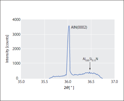
Fig. 2 XRD pattern in the 2θ-ω mode of the AlN/AlSiN layer of sample 2 separated from the 6H-SiC substrate.
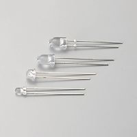
In order to confirm Si incorporation to the grown layers, EDS measurement was carried out. The profile of the peak intensity of Al and Si of a separated part of sample 2 as a function of the distance from the interface is shown in Fig. 3. Intense Si signal was detected in the region near the substrate and the signal gradually decreased. On the other hand, weak Al was detected at the interface and increased gradually. Note that the sensitivity is different for each element, so it does not mean Si content is higher than Al. This transition of Si and Al content agrees with the broad XRD peak around 36.5.The thickness of the transition layer is about 3μm.
For the non-separated region of sample 1, the Si content near the interface is estimated to be about 2% and the value is smaller than that of the separated region. This suggests that the Si incorporation and the formation of AlSiN play an important role in the separation of the grown layer and enough Si incorporation is necessary for the separation. The thickness of the transition layer is about 2.5 μm, which is almost same as the separated region. The distribution of the Si content of the separated region of sample 1 is considered to be similar to sample 2 from the XRD pattern, which shows a broad AlSiN peak with the highest Si content of 15%.
Si content in the grown AlN layers for both samples was very small and was inferred to be about 1% from the EDS profile. This is because the amount of Si in the source is small and the vapor pressure of Si is high enough, so Si in the source was exhausted in the initial stage of the growth.
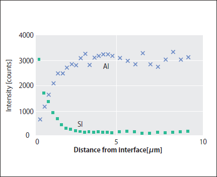
Fig. 3 EDS profile of Al and Si of a separated part of sample 2 from the AlSiN/SiC interface toward AlN surface.
The lattice constant a of AlSiN with the Si content of 15% is 0.314 nm, 7,8) which is larger than that of AlN, 0.311 nm. Therefore, the stress at the AlSiN/SiC interface is thought to be larger than AlN/SiC interface because the lattice constant a of 6H-SiC is 0.308 nm. We believe this causes easy separation of the grown AlN layer. Si content of the non-separated region was also measured by EDS and the content is smaller than that of the separated region as mentioned above. In this case, the lattice constant a of AlSiN is closer to that of AlN and the stress at the AlSiN/SiC interface is not large enough to separate. This also means that the difference in the lattice constants causes the separation. Of course the difference in thermal expansion coefficients is thought to play an important role in the separation, but the coefficient of AlSiN is not clear so far.
In summary, we demonstrated the separation of the AlN grown layer from the 6H-SiC substrate by the introduction of the AlSiN layer between AlN and 6H-SiC by adding Si powder to the source in sublimation growth. The Si content of the AlSiN layer of the separated sample is estimated to be 15%. This separation was probably caused by the lattice mismatch of SiC and AlSiN. We can easily obtain free-standing AlN by controlling the Si content of the AlSiN layer.
関連製品
論文を探す
今号では、各種の光源(半導体露光用EUV、複写機用LED、高輝度・長寿命・高安定のLDLS、光加熱用ハロゲンヒータなど)や、光の装置・システム(インターポーザ基板用露光装置、スマートフォン・タブレット端末用UVキュア、新規蛍光免疫素子Q-bodyによる薬物検出システムなど)など、2012年春から2013年春にかけて発表した技術や市場動向の論文15件を掲載しました。
シリーズ「大学研究室を訪ねて」では、新しい機能性タンパク質と有機メソッドの創製に挑む、東京工業大学資源化学研究所の上田先生をお訪ねし、開発に成功され、今、話題を集めているQ-bodyを用いた免疫測定法をご紹介しております。
(2013年06月)