(2017.10)
IMPACT
International Microsystems,Packaging,Assembly and Circuits Technology conference
New desmear process of organic substrate applications by Photodesmear technology
Shinichi Endo, Tomoyuki Habu, Hajime Kikuiri, Akira Aiba, Masaki Miura, Hiroki Horibe, Hiroko Suzuki, Shintaro Yabu†
Technology department 2, System solution division / Ushio Inc.
†: Equipment & systems semiconductor group / Ushio America, Inc.
1-90, Komakado, Gotemba city, Shizuoka, Japan (zip code 412-0038)
sn.endo@ushio.co.jp
ABSTRACT
Semi Additive process is considered to dry processing for the miniaturization of the semiconductor packages. There are many problems in the manufacturing substrate of print circuit board, at the materials, tools, processes, conditions etc. Wet process depends on the chemical reaction. That will reach a limit on the precision in the future. Dry process is a concept by semiconductor manufacturing process. But it is difficult to apply for print circuit board manufacturing process. Smear removal from via bottom and forming of surface roughness becomes the trade-off in the high end substrate production.
We have been conducted of the research and development of Photodesmear process as next generation process. Photodesmear is the technology that put decomposing organic matter by vacuum ultra violet light and removal inorganic matter by ultrasonic treatment together. The removal of smear on via bottom is controllable by quantity of the vacuum ultra violet light. In addition, Photodesmear can to divide a reaction of the smear removal and the roughness formation. We show our results of the improvement of adhesion between epoxy resin and copper by Photodesmear and dry seed process.
Integrated dry process is combined Photodesmear and sputter technologies for a view of panel level package process in the future. In addition, it has much possibility about the application to other processes. Integrated dry process provides many solutions of the next generation of semi additive process.
I. Introduction
Semi Additive process is a superior manufacturing method for print circuit broad. Semi Additive Process has a reasonable cost, and Semi Additive process realizes the fine line and space and narrow via pitch that is required by semiconductor industry rules. In recent years, the precision requirements have become smaller, while the miniaturization of the semiconductor and the shrinkage of the package size are demanded year by year.
In future fine line and space wiring, current Semi Additive process has some problems such as issues with slimming down of metal wiring in seed layer etching, adhesion between dielectric resin and Cu metal, defects of the resist pattern depend on wrong adhesion and, undercut of etching. Particularly, it is difficult challenge that the lower of the surface roughness to achieve high frequency electrical transmission loss is compatible with the improvement of the adhesion. The process of 2 microns line and space remains unusable. Dry process is proposed as alternative to wet process, which does not depend on chemical reaction and chemical solution penetration.
Recently wet desmear is limiting device miniaturization and dry process has been studied [1]. We have developed a new fundamentally desmear process applied with Vacuum ultra violet light (named Photodesmear process) from several years before [2-7].
From previous studies, we have shown that Photodesmear is effective in panel level sized samples. We have made these samples by formation of sputter seed layer and Cu electric plating. And we have shown good results of peel strength test and via connectivity test.
In this paper, we have reported the result by Photodesmear process about a detail of smear removal process. We have observed surface roughness forming by atomic force microscope. In addition, we have shown that other applications.
II. Direction to Photodesmear technology
Fig.1 shows the schematic mechanism of Photodesmear. The Vacuum ultra violet light (VUV: 172nm) has very high photon energy at 7.2eV which is capable of breaking bonds in organic molecular chains with molecular bonding energies lower than 172nm. The photons also serve to create ozone from atmospheric oxygen. Ozone has strong oxidization power; however the 172nm photon energy can further break down ozone to create excited state atomic oxygen which has oxidation power exceeding that of ozone. Ozone and excited state atomic oxygen then react with organic molecules that were decomposed to create H2O and CO2 [8-9].
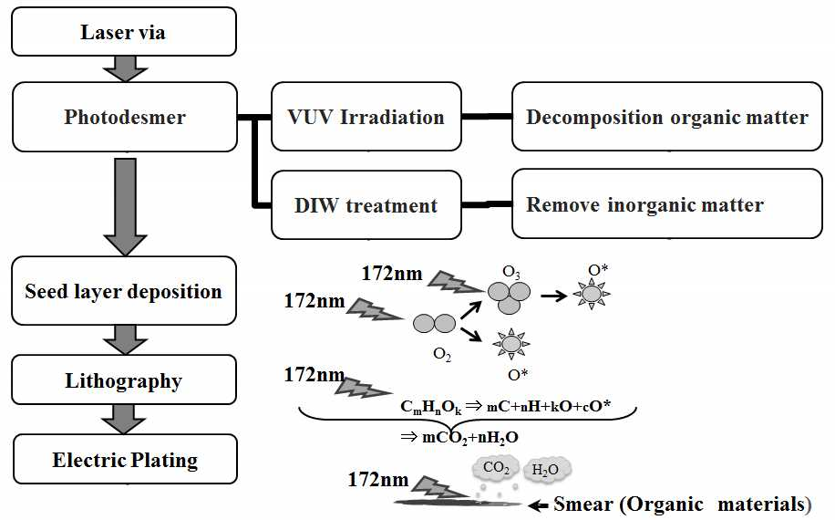
Fig. 1 Principle of Photodesmear process
The method of treatment of sample is as follows. The materials we used for this experiment are 400μm thick glass/epoxy core with CZ treated Cu film. Dielectric film (ABF-GX-T31, 25µm, provided by Ajinomoto Fine Techno Co., Inc.) is laminated with entire surface of the 500mm square panel. PET film is laminated on the surface of the dielectric material as protection layer.
Via holes were drilled by CO2 laser manufactured by Via Mechanics Ltd. (Model #: LUC2K21/1C) having φ50 micron diameter via with 1mm via pitch.
Fig.2 shows the cross section schematic diagram of a high-power VUV irradiation tool. The high-power Xenon excimer lamps which are newly developed are installed multiple to cover the irradiation area. A substrate is placed on the temperature controlled work stage. The process chamber is sealed and filled with the process gas. The VUV light (172nm) is irradiated through the synthetic silica glass window.
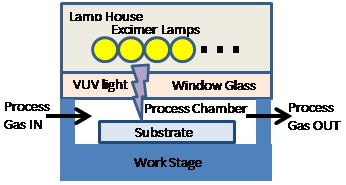
Fig. 2 Schematic diagram of VUV irradiation tool
After the organic matter decomposition by the VUV irradiation, ultrasonic cleaning by deionized water is provided to remove the silica filler.
Conventional process cannot handle desmear process with attaching a PET film to use strong chemicals, but Photodesmear can accomplished it. After Photodesmear, PET film was peeled off from dielectric surface.
A seed layer composed of Ti/Cu was sputtered on a panel. We have used a large sputtering tool made by Tango Systems Inc. “TOPAZ”. Pretreatment is necessary for an organic panel before sputtering the seed layer. The tool has necessary function for degas, ICP cleaner, etc., with optimized conditions of pretreatment. Therefore, followed to deposited 30 micron thickness of Cu layer by electric plating.
Via cleanliness and peel strength were evaluated by a pull test tool (Shimadzu EZ-LX). We used FE-SEM to determine the interfacing between Cu pads and filled via Cu. Surface roughness was measured by a laser microscope (Keyence Laser microscope VK-X160) and atomic force microscope (Keyence, Nano scale hybrid microcdopeVN-8010).
III. Experiment Results
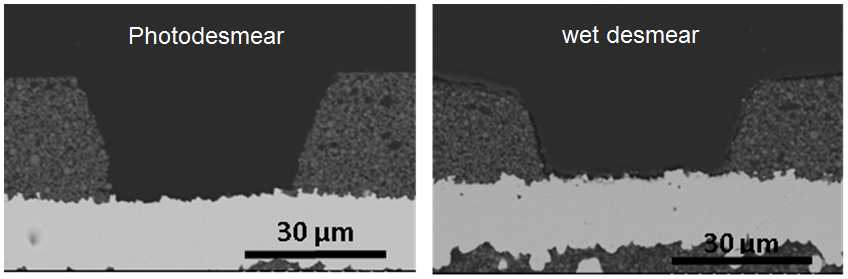
Fig. 3 shows SEM image of cross section of via that is comparison after desmear process. (a) is an after photodesmear process, (b) is an after wet desmear process.
(a) (b)
Fig. 3 Comparison of SEM image after desmear process.
When the via treated Photodesmear comperes the via treated wet desmear, Photodesmear has some advantages.Smear is removed cleanness. The surface of the dielectric resin is small. Via shape is kept, etc,.
(a) (b)
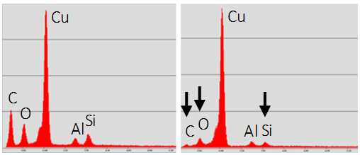
Fig. 4 EDX spectrum from via bottom
We observed a removal process of smear by EDX spectrum. (a) is typical spectrum before Photodesmear, (b) is after Photodesmear. The accelerated electron beam probe arrives at copper pad of via bottom. Therefore, we can measure residual quantity by the peak ratio (C/Cu) of the carbon for a copper strong signal.
Fig. 5 shows relations of irradiation time of vacuum ultra violet light and C/Cu. C/Cu decreases linearly for irradiation time. As for this thing, the reduction of C/Cu shows that it is the primary for quantity of the light.
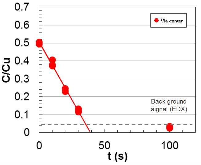
Fig. 5 Relations of VUV irradiation time and C/Cu
There is not it with the thing depending on a complicated chemical reaction such as the wet desmear. We can calculate quantity of removal of smear with quantity of the light, and design the desmear process.
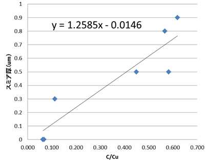
Fig. 6 Relations of C/Cu and smear thickness
We investigated relations of the C/Cu ratio and the smear thickness.It is difficult for the thickness of the smear to measure it. We measured average thickness of five points of center of via bottom from cross section SEM images in this report. From aresult of Fig. 5 and Fig. 6, the removal rate of smear by Photodesmear culclated with 11nm/s.
We can work to have left a poly ethylene terephthalate film for surface of the dielectric resin film by Photodesmear after CO2 laser drilling. It can not do the wet desmear. After Photodesmear, the surface roughness that a poly ethylene terephtarate film was peel off is very smooth.
When we laminates dry film resist for photo lithography, if roughness of the surface of seed layer is small, adhesion strength of dry film resist becomes a low. We can distribute cleaning of the via bottom and surface roughness control. We can get roughness neccesary for the adhesion of the dry film resist lamination. Fig.7 shows behavior of the roughness Ra at the irradiation time of additional vuv treatment. The roughness increase depending on vacuum ultra violet irradiation time, but become the constant value according to the size of the silica filler in a certain point. Photodesmear give flexibility for the formation of the surface roughness in production of the substrate. ( These data are different from the data of the laser microscope and atomic force microscope.)
Fig. 8 shows atomic force microscope images after additional vacuum ultra violet irradiation with some conditions.
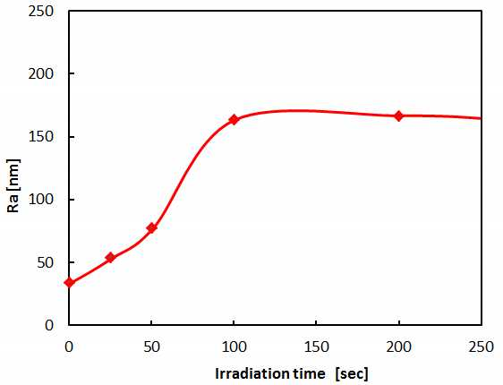
Fig. 7 Behavior of roughness Ra by the urradiation time
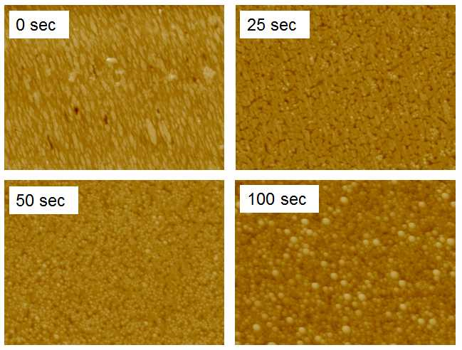
Fig. 8 AFM images of surface after additional vuv process
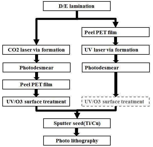
Fig. 8 Two type of the Photodesmear process
Ultra violet laser is the technology is effective for the micro via formation in next generation printed circuit board. It can form via which is smaller than CO2 laser, and the smear is little bit for example 1/5 degree. The wavelength of the UV laser is 355nm. When via is formed by UV laser, we cannot use poly ethylene terephthalate film. Because of ultra violet light is absorbed by PET film. However, the processing times become less than the CO2 laser. We can give surface roughness thinly, it is convenient.
We evaluated the peel strength of the Cu electric plating panel to confirm adhesion strength between dielectric and Cu layer.
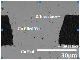
Fig. 9 cross section of via filled copper
Table 1 shows the peel strength of each condition. Conventional process means the peel strength data of a Wet desmear using KMnO4 followed by a dry seed layer with Cu plating. The peel strength of the Photodesmear with PET film for CO2 laser via processed panel was 0.70 kgf /cm. The peel strength of the Photodesmear without PET film for UV laser via processed panel was 0.51 kgf /cm, which suggests sufficient adhesion between the plated Cu and underlying dielectric surface and is higher than wet desmear with dry seed layer. Because there is not surface damage with the strong chemical solution, peel strength is improved by Photodesmear process.
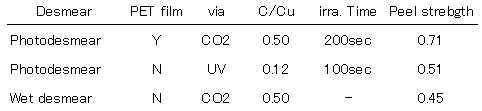
Table 1 Comparison of the condition and peel strength
IV. Conclusion
The dry process is a concept, which applies the wafer processing semiconductor production concept with the production for PCB packaging. Photodesmear process provides a solution for the problem that cannot be settled by the conventional process depending on a chemical reaction of the chemicals and diffusion of the chemical solution in the micro via.
In this study, Photodesmear process shows,
1) We showed principle of Photodesmear.
2) We investigated C/Cu EDX spectrum ratio and smear thickness, and led an etching rate.
3) We observed surface roughness and atomic force microscope images by additional vacuum ultra violet treatment.
4) We evaluated the peel strength in case of CO2 laser and UV laser.
Photodesmear separates the smear removal and a surface roughness formation process. Photodesmear offer possibility of the surface control in the production of the print circuit board. The principle has flexibility in future material development.
From these results, we confirmed that the dry process technology can meet next generation technical requirements of the next generation packaging technology. We will continue to investigate the Photodesmear process technological productivity and economic feasibility.
Ⅴ.Acknowledgment
A part of this experiment was supported with ABF-GX-T31 sample provided by Ajinomoto Fine-Techno Co., Inc.
Ⅵ.References
[1] John Y. Xie, “Developing High Density Packaging with Low Cost Stacking Solution” in SEMICON WEST 2013. October 2013.
[2] Tomoyuki Habu, “A Photo-Desmear Method for Via Residue Removal Using A VUV Light Source” in IMAPS 2013. October 2013.
[3] Hiroki Horibe, “A photo-desmear process using a VUV light source” in The Japan Institute of Electronics Packaging 2014. March 2014.
[4] Tomoyuki Habu, “Large Scale Photodesmear for Via Residue Cleaning in High Density Interconnect substrates” in IMAPS 2015, 48th International Symposium in Microelectronics. October 2015.
[5] Hiroko Suzuki, “Photodesmear Applicability for Blind Via Holes on a Build-up Substrate” in The Japan Institute of Electronics Packaging 2016. March 2016.
[6] Masahito Namai, “Full-sized Panel Photodesmear for Via Residue Cleaning” in IEEE2016 Electric Components and Technology Conference, June 2016
[7] Shinichi Endo, “Improvement of Coherency of the Panel Level Package by Integrated Dry Process” in IMAPS 2016 49th International Symposium in Microelectronics. October 2016
[8] Shinichi Endo, “ UV Cleaning” in Electronics Cleaning Technology. Technology Information Association. Oct 2007.
[9] Nobuyuki Hishinuma, “Excimer Photon Source” in Electrical Journal 2001 FPD Technology