The Institute of Electronics, Information and Communication Engineers (IEICE)
28th International Semiconductor Laser Conference
(2022)
Passive waveguide loss measurements in an InGaN-based laser diode structure
Atsushi A. Yamaguchi1, Kenta Ogasawara1, Shigeta Sakai2, Tadashi Okumura2, and Koichi Naniwae2
1Kanazawa Institute of Technology, Optoelectronic Device System R&D Center, Ohgigaoka 7-1, Nonoichi-City, Japan
2Ushio Inc., 1-90 Komakado, Gotemba, Shizuoka, 412-0038, Japan
Abstract
Waveguide loss spectrum in an InGaN laser diode (LD) has been measured and the results were compared with an InGaP LD. It is observed that the spectrum has a long tail in the InGaN LD while it shows a sharp rise in the InGaP LD.
I.Introduction
InGaN quantum-well (QW) structures are widely used as active layers in violet, blue and green LEDs and laser diodes (LDs). Light-emitting devices using the InGaN-QW active layers have potential of covering entire visible light wavelength range by controlling InGaN alloy composition. It is, however, difficult to grow InGaN QW layers with spatially uniform alloy composition. This inevitable alloy fluctuation has strong effects on optical properties and device characteristics of LEDs and LDs. It has been reported that the non-radiative recombination processes are suppressed in such fluctuated active layers because carrier mobility is suppressed by the fluctuation and the probability of carrier capture to the defects can be significantly suppressed [1-3]. It has been also reported that the optical gain peak is broaden and differential gain decreased due to the tailing of density of states (DOS) by the fluctuation [4-6]. The DOS tailing can enhance the absorption coefficient below energy gap and can increase the passive waveguide loss in InGaN-based LD structures, but there is only a few reports on waveguide loss spectrum in such LD structures. In this study, we have measured passive waveguide loss spectrum in an InGaN-QW LD. The spectrum has been also measured in a conventional InGaP-QW LD for comparison, which has very homogeneous active layers.
II.Experimental
Figure 1 shows a schematic diagram to explain the principle of the waveguide loss measurement [7-8]. When excitation light is focused on the sample surface by object lens at the position where the distance from the sample edge is R, photoluminescence (PL) light propagates in the waveguide by distance R and emits from the edge. Since a part of the light is absorbed in the waveguide, the edge emission intensity and spectrum will depend on the distance R. The light absorption can be described by the following expression:
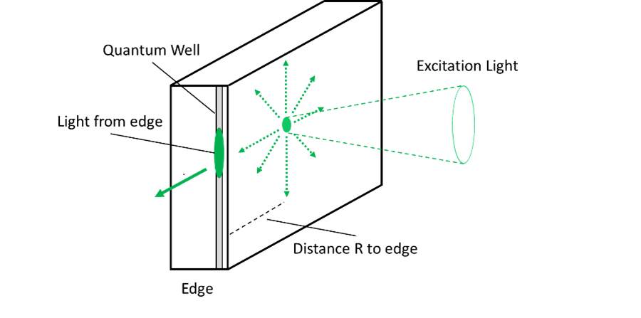
Fig.1 A schematic diagram to show the principle of the waveguide loss measurements in laser diode structures.
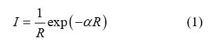
where I is the light intensity of edge emission, and α is the absorption (or loss) coefficient of the waveguide. In this measurement, edge emission intensity & spectrum were measured as functions of distance R, and absorption (loss) coefficient was calculated by Eq. (1) for each wavelength in the QW emission peak. In this study, we measured the waveguide loss spectrum for an InGaN-QW LD structure. The loss spectrum for a conventional AlInGaP red-light-emitting LD structure was also measured for comparison.
III.Results and Discussions
Figures 2(a) and 2(b) show edge emission spectra for the InGaP LD and InGaN-QW LD samples as a function of the distance R.
The emission intensity (I) is multiplied by the distance R, and the I x R spectra are plotted in the figures because the I x R is proportional to exp(-αR) in Eq. (1). A decease in the values of I x R and a red shift of the emission with the increase of distance R are clearly observed, in the figures, for both the samples. These results indicate that the emission light is absorbed in the waveguide and that the absorption coefficient is larger in the shorter wavelength region.
Figures 3(a) and 3(b) show measured waveguide loss spectra (red circles) for an InGaP LD and an InGaN-QW LD. The photoluminescence (PL) spectra from sample surface (green solid line) and sample edge [R = 200 µm] (violet broken line) are also plotted. It is observed that PL peak position difference between the surface and edge emissions is very large (~ 200 meV) in the InGaN LD sample while there is almost no difference in the AlInGaP LD sample. In addition, the absorption coefficient gradually rises from an energy much lower than the PL peak energy of surface emission in the InGaN LD sample while the coefficient sharply rises at nearly PL peak energy in the InGaP LD sample. These results show that the InGaN QW has a large DOS tailing while the InGaPQW has a step-like DOS.
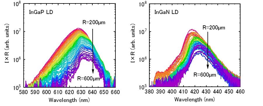
Fig. 2 Edge emission spectra in (a) the InGaP LD and (b) InGaN-QW LD samples are shown for various distance
R. The emission intensity (I) is multiplied by the distance R, and the I x R spectra are plotted in the figures.
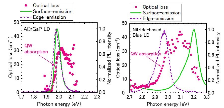
Fig. 3 Measured surface-emission (green solid line) and edge-emission (violet broken line) spectra of (a) the
InGaP-QW LD and (b) InGaN-QW LD. Waveguide optical loss spectra (red circles) are also plotted.
IV.Conclusions
We have measured waveguide loss spectrum for an InGaN-QW laser diode structure. The loss spectrum for a conventional InGaP-QW red-light-emitting LD structure was also measured for comparison. It is observed that PL peak position difference between the surface and edge emissions is very large (~ 200 meV) in the InGaN LD sample while there is almost no difference in the InGaP LD sample. In addition, the absorption coefficient gradually rises from an energy much lower than the PL peak energy of surface emission in the InGaN LD sample while the coefficient sharply rises at nearly PL peak energy in the InGaP LD sample. These results show that the InGaN QW has a large waveguide loss.
References
[1] Y. Narukawa, S. Saijo, Y. Kawakami, Sz. Fujita, Sg. Fujita, and S. Nakamura, J. Cryst. Growth 189/190 (1998) 593.
[2] S. Chichibu, K. Wada, and S. Nakamura, Appl. Phys. Lett. 71 (1997) 2346.
[3] T. Mukai, D. Morita, and S. Nakamura, J. Cryst. Growth 189/190 (1998) 778.
[4] A. A. Yamaguchi, M. Kuramoto, A. Kimura, M. Nido, and M. Mizuta, Jpn. J. Appl. Phys. 40 (2001) L548.
[5] A. A. Yamaguchi, M. Kuramoto, M. Nido, and M. Mizuta, Semicond. Sci. Technol. 16 (2001) 763.
[6] M. Kuramoto, Y. Hisanaga, A. Kimura, N. Futagawa, A. A. Yamaguchi, M. Nido and M. Mizuta, Semicond. Sci. Technol. 16 (2001) 770.
[7] P. C. Mogensen, P. M. Smowton, and P. Blood, Appl. Phys. Lett. 71, (1997) 1975.
Dmitry S. Sizov, Rajaram Bhat, Albert Heberle, Kechang Song, and Chung-en Zah, Appl. Phys. Express 3 (2010) 122104.