光技術情報誌「ライトエッジ」No.24(2002年4月発行)
2001 International Conference on Solid State Devices and Matelials,
Extended Abstracts of the 2001 International Conference on Solid State Devices and Materials,Tokyo,2001,pp.520-521
(2001年9月)
C-8-1
Novel PZT Crystallization Technique by Using Flash Lamp for FeRAM Embedded
LSIs and 1Tr FeRAM Devices
Koji Yamakawa, Keitaro Imai, Osamu Arisumi, Tsunetoshi Arikado,1Masaki Yoshioka,
1Tatsushi Owada and Katsuya Okumura
Process & Manufacturing Engineering Center, Toshiba Corp., Semiconductor Company
8, Shinsugita-cho, Isogo-ku, Yokohama 235-8522, Japan
Phone:+81-45-770-3675 Fax:+81-45-770-3577 E-mail: koji.yamakawa@toshiba.co.jp
1Lamp Technology & Engineering Division, Ushio Inc.
1194, Sazuchi, Bessho-cho, Himeji, Hyogo 671-0224, Japan
1.Introduction
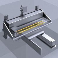
FeRAM embedded LSIs have potential for use in multifunctional IC cards, RF cards, memory embedded micro controllers etc.. However, capacitor degradation during ILD CVD and RIE processes and cross contamination problems during device integration have been reported. Formation of ferroelectric capacitors on top of Al wiring is a way to overcome the problems. Furthermaore, 1Tr (transistor) type FeRAM is a candidate to make a high density Gbit memory. It is significant to form ferroelectric films on transistor gates without interface degradation. In order to achieve the devices suppression of thermal damage to the substrates is essential. We have developed an ultimate rapid thermal process called flash lamp process to crystallize PZT films (Fig.1).
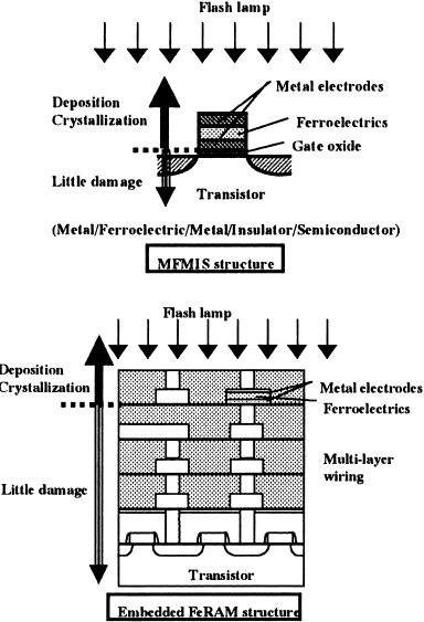
Fig.1 Concept of PZT crystallization by flash lamp for MFMIS structures and FeRAM embedded ones.
2.Experimental
An experimental flash lamp apparatus is shown in Fig.2. Flash Xe lamp tubes were installed with a reflector above a substrate stage with a heating system. Total current and flash lamp pulse can be controlled by capacitors and inductors. The typical current to the tubes was 1800A max. (27J/cm2) with 1.0-1.5msec. pulse width. In order to promote PZT crystallization substrate temperature was elevated to 300-400°C. The PZT films used here were amorphous ones prepared by RF magnetron sputtering at ambient temperature. Pt or SiO2 deposited Si substrates were used.
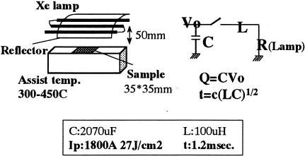
Fig.2 Exeperimental setup.
3.Results and discussion
Firstly, PZT crystallization was tried on Pt coated Si substrates. Parameters such as flash lamp energy density (almost proportional to the current), lamp irradiation time and substrate temperature, that we call assist temperature, were changed to see basic PZT crystallization behavior. The crystallization was found to start at 350°C with flash lamp output energy of 27J/cm2. In the case of no irradiation at elevated assist temperatures up to 450°C no perovskite phase was obtained. Figure 3 shows phase transition behavior from the results of XRD. Microstructures of PZT films prepared by using the flash lamp process at various assist temperatures are exhibited in Fig.4. when the films were crystallized by flash lamp granular PZT grains were obtained that were different from normally RTA-crystallized films with columnar structures. This is probably due to homogenious crystallization mechanism by the irradiation and impulse thermal process. The films show random orientation not along <111> even on (111) oriented Pt films. The results also say that amorphous PZT can transform to perovskite ferroelectric phase for a very short period of time like 1msec.. An example of electrical properties is shown in Fig.6. The capacitor has a Ru top electrode followed by 350°C furnace annealing to form a good top electrode interface.
Secondly, PZT crystallization was carried out on SiO2. It has been recognized that it is hard to form PZT on SiO2 except for PbTiO3 because of serious diffusion and reactivity between Pb based material and SiO2. However, we prepared well-crystallized PZT films without SiO2 interface degradation. In Fig.5 comparison between flash lamp crystallized PZT and no flash processed one is shown. By application of flash lamp PZT can be crystallized on SiO2. In 1 Tr FeRAM devices, less degradation at ferroelectric/SiO2 interfaces is important to control the transistor gate.
Lastly, PZT formation on Al wiring layers and effects of flash lamp pulse train were investigated. Figure 7 shows crystallized PZT films on Al wiring. No degradation of Al was observed. As displayed in Table 1 a cumulative effect of flash lamp irradiation is shown. Increase of shot number promotes PZT crystallinity. This data can lead to optimize flash lamp condition from view points of lamp life and flash lamp system design.
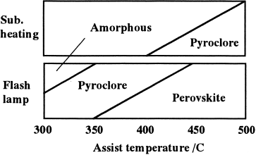
Fig.3 Phase transition of PZT films with flash lamp treatment and no flash lamp heating.
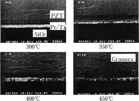
Fig.4 Microstructures of PZT films on Pt crystallized by flash lamp at various assist temperatures.
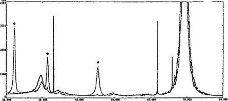
Fig.5 XRD patterns of PZT films formed on SiO2. (Dot: Perovskite phase for flash irradiated sample)
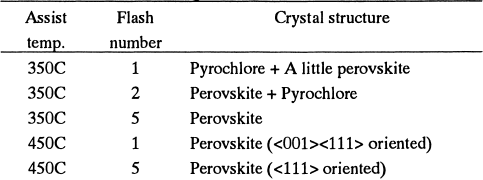
Table I: Effect of pulse number on PZT formation
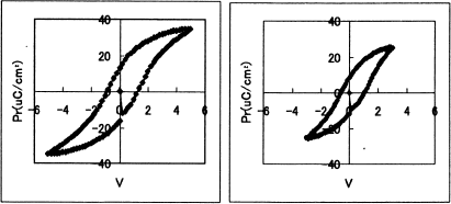
Fig.6 Hysteresis loops of Pt/PZT/Ru capacitor.
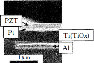
Fig.7 Crystallized PZT on Al wiring layer. (No damage to the substrateobserved)
4.Conclusions
Potential of flash lamp process to crystallize PZT films was shown without damage to the substrates. This technique enable PZT formation on SiO2 and Al wiring layers showing possibility of FeRAM embedded LSIs and 1Tr type FeRAM devices.
関連製品
論文を探す
各社との共同研究成果を含む学会発表、専門誌への投稿、さらに共同研究で関連した他社論文発表で特に関係の深いもの、また、ウシオで開催された講演会などをご紹介しています。
(2002年04月)