光技術情報誌「ライトエッジ」No.24(2002年4月発行)
2001 International Conference on Solid State Devices and Matelials
(2001年9月)
High-Performance Low-k Dielectric using Advanced EB-Cure Process
Miyoko Shimada, Hideshi Miyajima, Rempei Nakata and Takashi Yoda
TOSHIBA CORPORATION SEMICONDUCTOR COMPANY
8, Shinsugita-cho, Isogo-ku, Yokohama 235-8522, Japan
Phone: +81-45-770-3520 Fax: +81-45-770-3568 E-mail: mi-yamada@amc.toshiba.co.jp
1. Introduction
The integration of the multilevel interconnection by damascene Cu with low-k dielectrics is the key technology for logic devices. Fundamental requirements include: high mechanical strength of low-k material to avoid the crack of film and scratch by CMP process, and lower thermal budget in order to control the grain growth and the diffusion of Cu. In general, the coated low-k film has poor mechanical properties. For the current formation of low-k spin-on dielectrics, 30-60 minutes is needs to be cured at 400°C, after the film coating and pre-baking. In this paper,we will present the impact of the EB cure process for0.10µm-nodes multilevel interconnect technology.
2. Experimental
LKDTM material (JSR Corporation), ladder-type MSX(poly-methylsiloxane) low-k dielectric (k = 2.9), was used in this work. Samples were coated and prebaked at 80°C and 200°C in succession for 1minute, followed by EB cure process.
The EB cure chamber has a dry pump and a gas supply unit, a heating single-wafer stage that controls up to 500°C and an EB unit including 19 EB tubes (Miniature Electron Tube Min-EB UEB-04: USHIO INC.).
The EB cure process was carried out as following conditions; 25keV of accelerating voltage, 400°C of the wafer temperature and 10 Torr (in N2) of pressure in process chamber. Total dose and the dose rate are variable appropriate for the purpose. For these conditions, the thickness and refractive-index uniformity of EBcured LKDTM film were very reasonable. In the following chapter,we will discuss the film properties for each EB cure condition (total dose and dose rate), comparing with thermal cure condition of 400°C for 30minutes using the only hot-plate (HP).
3. Results and discussion
Figure 1 shows the modulus and dielectric constant for EB cured film as a function of dose. The modulus E, which is measured using the nanoindentation technique, has been1.9 times bigger at 500µC/cm2 and 2.8 times bigger at1000µC/cm2 , as compared with the value of thermal cured film (E=8.1GPa). The improvement in mechanical strength induced 1/1000 or less velocity of a crack propagation in EB cured film, as compared with thermal cured film.Figure 2 shows the modulus and dielectric constant for EB cured film as a function of cure time, whicn is determined by dose rate. In Fig. 2, total dose is fixed at 500µC/cm2 ,with respect to lower thermal budget. As can be seen in Fig.2, EB cure needs shorter process time as 5 minutes to obtain the same k value of thermal cured film. Table 1summarizes the properties of EB cured film against conventional HP cured one. It is remarkable that EB cure process is drastically effective in improving the mechanical strength of LKDTM film and reducing thermal budget.
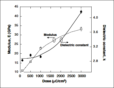
Figure. 1 The modulus and dielectric constant for EB cured film as a function of dose. Modulus: square and broken line.Dielectric constant: solid circle and line.
Concerning the structure of EB cured LKDTM film, both peak split around 1130cm-1 for Si-O bond streching and peak intensity at 1270cm-1 for Si-CH3 bond decrease with increasing dose, as shown in Figure 3, which indicates FT-IR spectra for EB cured and thermal cured film. It means that Si-CH3 bonds are broken up by EB and Si-O random-network are reconstructed. On the other hand the result of RBS analysis evidenced that carbon content in film don’t change by the EB irradiation. In addition, the result of FT-IR analysis exhibited an existence of the polymer-like clusters with C-C bond, namely EB cured film has a hybrid structure between a SiO2 -based siloxane and carbon-based polymer. We believe that the properties of EB cured LKDTM film is derived from this hybrid structure.
As for the integration with EB cured LKDTM film, we confirmed the restraint of gas penetration during ashing process, and equality in dry etching properties between EB cured film and conventional HP cured one. Figure 4 shows trench etch profile of EB cured and thermal HP cured film.Both films exhibit same characteristic. Further investgations are in progress.
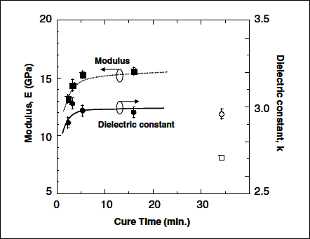
Figure. 2 The modulus and dielectric constant for EB cured film as a function of cure time. Total dose is 500 オ C/cm2Modulus: square and line. Dielectric constant: solid circle and line.
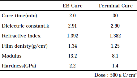
Table 1 Film Characteristic Comparison
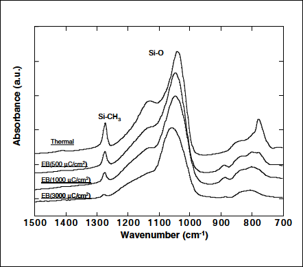
Figure. 3 FT-IR spectra for EB cured and thermal cured film.
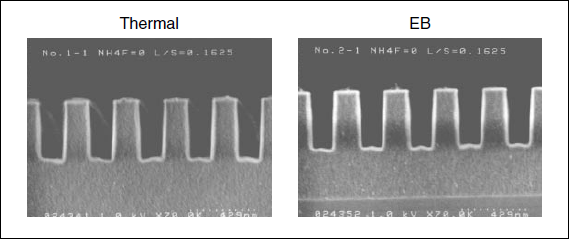
Figure. 4 Trench etch profile of EB cured and thermal cured film.L/S=0.1625µm.
4. Conclusion
We developed the EB cure process for low-k dielectrics.For JSR LKDTM film, the mechanical strength becomes 1.9times stronger than conventional HP cured film, and cure time is shortened from 30 minutes in 5 minutes. These results show that the EB cure technique for the coated low-k film will be very useful in the LSI processes. Further the EB cure technology has possibility to apply to the other materials (ex. SOG, Photo resist etc.) for the LSI fabrication processes.
Acknowledgments
We would like to express our sincere thanks to Dr. K.Okumura, Dr. N. Hayasaka, Dr. M. Miyoshi and Dr. T.Nakasugi for their helpful suggestions, and also to H.Masuda for his assistance.
論文を探す
各社との共同研究成果を含む学会発表、専門誌への投稿、さらに共同研究で関連した他社論文発表で特に関係の深いもの、また、ウシオで開催された講演会などをご紹介しています。
(2002年04月)