光技術情報誌「ライトエッジ」No.29(2007年8月発行)
2006.9 21st European Photovoltaic Solar Energy Conference
A NEW TYPE POLY-Si PREPARED BY FAST LAMP ANNEALING
OF Cat-CVD a-Si AND ITS DEFECT PASSIVATION
BY HIGH PRESSURE WATER VAPOR ANNEALING
Hideki Matsumura1, Keisuke Ohdaira1, Makoto Fukuda1, Yuki Abe1, Noritaka Usami2, Kazuo Nakajima2,
Takeshi Karasawa3, and Tetsuya Torikai3
1 Japan Advanced Institute of Science and Technology (JAIST), 1-1 Asahidai, Nomi, Ishikawa 923-1292, Japan
2 Institute for Materials Research (IMR), Tohoku University, 2-1-1 Katahira, Sendai, Miyagi 980-8577, Japan
3 R&D Center, Ushio Inc., 1194 Sazuchi, Bessho-cho, Himeji, Hyogo 671-0224, Japan
TEL : +81-761-51-1563, FAX : +81-761-51-1149, E-mail : ohdaira@jaist.ac.jp
ABSTRACT
Nano-grain poly-Si (ngp-Si) films, which is a new type polycrystalline Si consisting of dense small grains with diameters of several ten nm, has been successfully fabricated by rapid thermal annealing (RTA) both for several ten seconds and for less than ten milliseconds. High pressure water vapor annealing (HPWVA) is found to be effective to terminate dangling bonds in ngp-Si films and can drastically decreases their defect densities down to the order of 1016/cm3. Silicon nitride (SiNx) films deposited on a-Si films act to suppress desorption of hydrogen atoms during RTA, resulting in lowering the defect density of ngp-Si as well. An ngp-Si film annealed for several milliseconds indicates a minority carrier lifetime of 5-10µs after HPWVA, showing the potential for high-efficient thin-film solar cell materials.
Keywords
Crystallization, Defect Density, Lifetime, Micro Crystalline Si, Passivation, Rapid Thermal Processing
1 INTRODUCTION
Microcrystalline Si (µc-Si) films formed by deposition techniques such as plasma-enhanced chemical vapor deposition (PECVD) and catalytic CVD (Cat-CVD) have been widely used for thin film solar cells. However, highly crystallized µc-Si tends to absorb oxygen atoms into the grain boundaries, resulting in degradation of the electrical properties. To avoid this problem, µc-Si films containing amorphous Si (a-Si) in the grain boundaries are unwillingly used for current µc-Si solar cells. However, such remaining a-Si is unfavorable for highefficient solar cell materials since it reduces minority carrier diffusion length and causes light-induced degradation
Therefore, as a novel material for high-efficient µc-Si solar cells, we have studied nano-grain poly-Si (ngp-Si), consisting of dense small grains with diameters of less than 100 nm [1, 2]. It has been clarified that the ngp-Si films can be formed by rapid thermal annealing (RTA) of a-Si films for several ten seconds and no oxygen absorption can be observed in Fourier transform infrared spectroscopy (FT-IR) after exposure to atmosphere for several days [2]. However, considering the practical application for high efficient solar cells, RTA should be performed within much shorter time in order to suppress damage to glass substrates, and serious dopant diffusion. Furthermore, defect density increases from less than 1x10¹⁶/cm3 to around 1x10¹⁸/cm3 due to desorption of hydrogen atoms during RTA. Hence, effective defect passivation process for ngp-Si films should be also studied.
In this study, we have investigated fundamental properties of ngp-Si films fabricated by RTA for several ten seconds and for less than ten milliseconds. Defect reduction techniques using high pressure water vapor annealing (HPWVA) and silicon nitride (SiNx) capping have also been attempted to realize low-defect ngp-Si films applicable for high-efficient thin film solar cells.
2 EXPERIMENTAL
2.1 Formation of ngp-Si films
For deposition of a-Si films, we used Cat-CVD method. This method is favorable for fabrication of ngp-Si films since a-Si films with hydrogen content of as low as 3% can be formed and thus desorption of hydrogen during annealing is unlikely to occur. The temperatures of tungsten catalyzers and quartz substrates during deposition were 1750°C and 250°C, respectively. The film thickness was systematically changed from 100 nm to 1500 nm. For fabricating ngp-Si, RTA was performed both for several ten seconds and less than ten milliseconds.
2.2 Defect passivation
Some of a-Si films were covered with SiNx films deposited by Cat-CVD method in order to avoid hydrogen desorption during RTA. HPWVA was performed under pressure from 0.2 to 3.0 MPa and temperature up to 350°C. The capping SiNx films were removed by H3PO4 boiling before HPWVA. The process flows of defect passivation for ngp-Si films are summarized in Fig. 1.
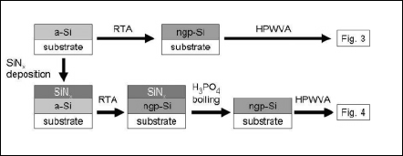
Figure 1: Process flows of defect passivation for ngp-Si films.
2.3 Characterization of ngp-Si films
The grain sizes in ngp-Si films were characterized by scanning electron microscopy (SEM) images as well as X-ray diffraction (XRD) patterns. Degree of crystallization of ngp-Si films were evaluated by Raman spectroscopy. Defect densities of ngp-Si films before and after passivation process were estimated by electron spin resonance (ESR). Minority carrier lifetimes of ngpSi were measured by microwave photoconductivity decay (µ-PCD) method. The sample surfaces were passivated by ethanol-iodine solution during the measurement.
3 RESULTS AND DISCUSSION
3.1 Ngp-Si films fabricated by normal RTA
Figure 2 shows cross-sectional SEM images of ngp-Si films. Numbers of small grains are closely packed from bottom to top of the film. These figures show that whole a-Si films can be successfully transformed to ngpSi by RTA. The grain size is estimated to be about 50 nm, which is approximately in agreement with that estimated by Scherrer’s equation from XRD patterns. A series of Raman spectra of ngp-Si films were summarized in elsewhere [1, 2].
Figure 3 shows HPWVA temperature dependence of defect density of ngp-Si films with various thicknesses performed for 1 hour under 0.2 MPa. The defect densities, initially around 5 x 10¹⁷ /cm3, can be effectively decreased down to around or lower than 1 x 10¹⁶ /cm3 when HPWVA temperature increases up to 350 °C. This result also shows that the defect density of ngp-Si after HPWVA is sensitive to temperature, which is probably because diffusion of terminating atoms into ngp-Si are enhanced and thus defects located far from the surface start to be terminated.
Figure 4 indicates defect density of ngp-Si films with various ngp-Si and SiNx film thicknesses. HPWVA performed at 350 °C under 0.2 MPa. Drastic reduction of defect densities occurs for all the ngp-Si films when Si films are capped by SiNx films. The defect density can be decreased down to 2 x 10¹⁶/cm3 for ngp-Si films with a thickness of 500 nm and to 6 x 10¹⁶ /cm3 even for 1000 nm-thick ngp-Si films. This indicates that desorption of hydrogen atoms in Si films during RTA has been effectively suppressed by SiNx film capping. There may be another effect that hydrogen atoms contained in SiNx films diffuse into ngp-Si films and terminate dangling bonds in them during RTA.
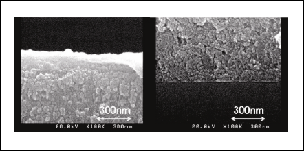
Figure 2: Cross-sectional SEM images for an ngp-Si film in top and bottom areas. Small grains with diameters of several ten nm are seen in both parts.
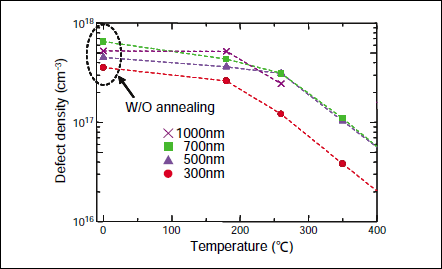
Figure 3: Defect density of ngp-Si films for various film thickness as a function of HPWVA temperature.
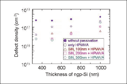
Figure 4: Defect density of ngp-Si films with and without SiNx capping and/or HPWVA.
3.2 Ngp-Si films fabricated by millisecond RTA
Figure 5 shows Raman spectra of Si films after millisecond RTA under the same annealing condition. The spectrum of 100 nm-thick film holds a broad peak originating from a-Si phase around 480 cm-1 even after RTA, whereas that of 1500 nm-thick film has a sharp peak located at 520 cm-1 indicating crystallization of the film. These results show that thicker film tends to be crystallized under lower lamp intensity, which is probably because this millisecond process is performed in nonthermal equilibrium unlike the case of normal RTA condition and majority of heat intensively generated in the surface region is easier to escape into a substrate in case of thinner Si films. Same phenomena have also been observed in another investigation [3]. This tendency is rather prefer to application for thin film solar cells which needs optical absorption layer with a thickness of at least several µm for sufficient absorption of sunlight.
Figure 6 indicates the grain size of poly-Si films fabricated by millisecond RTA as a function of relative lamp intensity estimated from XRD patterns. As lamp intensity increases, the grain size also gradually increases. However, they are still in the order of several ten nm and thus ngp-Si structures are probably formed.
Figure 7 shows the result of µ-PCD measurement for a ngp-Si film with a thickness of 1500 nm after HPWVA under 3.0 MPa at 350°C. High minority carrier lifetime of 5-10µs can be observed. Assuming the minority carrier mobility of 10 cm2/Vs, which is equivalent to the measured majority carrier mobility of ngp-Si, this lifetime corresponds to the minority carrier diffusion length of over 10µm. No significant signal can be observed without HPWVA. Therefore, HPWVA is also effective for ngp-Si films fabricated by millisecond RTA and essential process for high-quality ngp-Si films applicable for thin film solar cells.
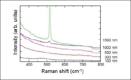
Figure 5: Raman spectra for Si films with various thickness after millisecond annealing. Gradual increase of each spectrum in small wavenumber region indicates Rayleigh scattering.
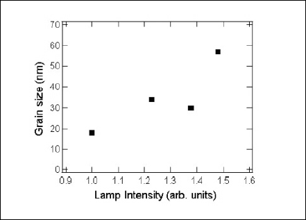
Figure 6: Grain size of ngp-Si films as a funciton of relative lamp intensity.
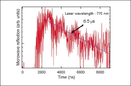
Figure 7: Minority carrier lifetime of ngp-Si after HPWVA.
4 CONCLUSIONS
In this study, we have investigated effective passivation techniques for ngp-Si films. HPWVA is found to be effective for defect passivation of ngp-Si films. Capping by SiNx films before RTA can also decreases defect density and these combination can yields defect density of ngp-Si of 2 x 10¹⁶/cm3 for optimum condition.
Millisecond RTA has also newly attempted and the ngp-Si films with a thickness of 1500 nm have been successfully formed. The µ-PCD measurement yields the minority carrier lifetime of the ngp-Si films of 5-10µs, showing high capability for high-efficient thin film solar cells.
ACKNOWLEDGMENTS
This work is partially supported by NEDO through PVTEC.
関連製品

論文を探す
フラッシュランプを用いた瞬間熱処理技術の関連論文を中心に、2006年に各学会や研究会で発表した論文13件、専門誌への投稿論文4件をご紹介します。
(2007年08月)