光技術情報誌「ライトエッジ」No.29(2007年8月発行)
2006.10 4th International Conference on Hot-Wire CVD(Cat-CVD)Process
Poly-Si Films with Long Carrier Lifetime Prepared by Rapid
Thermal Annealing of Cat-CVD Amorphous Silicon Thin Films
Keisuke Ohdaira1 Yuki Abe1, Makoto Fukuda1, Shogo Nishizaki1, Noritaka Usami2, Kazuo Nakajima2,
Takeshi Karasawa3, Tetsuya Torikai3 and Hideki Matsumura1
1Japan Advanced Institute of Science and Technology (JAIST), 1-1 Nomi, Asahidai, Ishikawa 923-1292, Japan
2Institute for Materials Research, Tohoku University, 2-1-1 Katahira, Aoba-ku, Sendai, Miyagi 980-8577, Japan
3R&D center, Ushio Inc., 1194 Sazuchi, Bessyo-cho, Himeji, Hyogo 671-0224, Japan
Abstract
Polycrystalline silicon (poly-Si) films thicker than 1.5µm consisting of dense small grains called nano-grain poly-Si (ngp-Si) are formed by flash lamp annealing (FLA) of amorphous silicon (a-Si) films formed by catalytic chemical vapor deposition (Cat-CVD) method. Crystallinity of the ngp-Si films can be controlled by changing lamp irradiance. Secondary ion mass spectroscopy (SIMS) profiles of dopants in the ngp-Si films after FLA shows no serious diffusion. A minority carrier lifetime of over 5µs is observed from these ngp-Si films after defect termination process using high pressure water vapor annealing (HPWVA), showing possibility of application for high-efficient thin-film solar cells.
Keywords
Annealing, Crystallization, Raman scattering, secondary ion mass spectroscopy (SIMS), Silicon, Solar cells, Microcry stalline, Minority carrier lifetime
1. Introdution
Microcrystalline Si (µc-Si) is an attractive material for high-efficient solar cells since it has no light-induced degradation unlike a-Si films. However, µc-Si for thinfilm solar cells formed by deposition techniques such as plasma-enhanced chemical vapor deposition (PECVD) and catalytic CVD (Cat-CVD) are not be completely crystallized. This is because absorption of oxygen atoms into grain boundaries, which deteriorates electronic properties of µc-Si films, is suppressed by remained amorphous Si (a-Si). However, photo-generated carriers have to path through a-Si, leading to serious reduction of diffusion length.
On the other hand, poly-Si films formed by rapid thermal annealing (RTA) of a-Si films prepared by Cat-CVD with hydrogen content of lower than 3% show no oxygen diffusion and thus have high carrier mobility of several ten cm2/Vs[1]. We named this special poly-Si nano-grain poly-Si (ngp-Si). The dangling bonds generated due to desorption of hydrogen atoms can be effectively terminated by high pressure water vapor annealing after RTA[2]. However, for fabrication of high-efficient thin-film solar cells using this ngp-Si films, crystallization time should be reduced down to about 10 milliseconds in order to avoid serious dopant diffusion as well as to suppress thermal damage to glass substrates.
Flash lamp annealing is a millisecond treatment using lamp irradiation with broad spectrum in visible range and thus can be a candidate for a new process to form ngp-Si films and to fabricate ngp-Si solar cell structures. There have been some reports for crystallization of amorphous Si (a-Si) with thickness of several hundred nm or less aiming to apply them to thin-film transistor[3], whereas no reports for formation of crystallized films over 1µm for the purpose of application to solar cells.
In this study, we have investigated crystallization of Cat-CVD a-Si films over 1µm by FLA. Their fundamental properties such as dopant diffusion and minority carrier lifetime of the formed films have also been investigated.
2. Experiments
Intrinsic a-Si thin films as precursors having thickness from 100nm to 1500nm were formed by Cat-CVD method on quartz substrates. Tungsten wires heated at 1750°C were used as catalyzers. Quartz substrates were heated at 250°C during deposition. The hydrogen contents of deposited a-Si films estimated by FT-IR measurements are about as low as 3%, resulting in low hydrogen desorption during FLA. For investigation of dopant diffusion, p-i-n structures with each thickness of 20nm, 700nm, and 20nm, respectively, were also formed in this order on SnO2 films formed on glass substrates. Diborane (B2 H6 ) and phosphine (PH3) gases were used to form p- and n-type a-Si layers, respectively.
The treatment time of FLA was fixed at less than 10 milliseconds, while its irradiance was systematically changed. HPWVA was performed to some of films after FLA under 3 MPa and 350°C in 60 min. The impurity profiles for p-i-n structures before and after FLA were observed by secondary ion mass spectrometry (SIMS). Fundamental properties of the films were characterized by X-ray diffraction (XRD), Raman spectroscopy and UV-transmission measurements. Minority carrier lifetimes were measured by microwave photo-conductivity decay (µ-PCD) with an excitation laser wavelength of 770 nm.
3. Results and discussion
Raman spectra of films having a thickness from 100 nm to 1500 nm after FLA are summarized in Fig. 1. Broad peaks centered at 480cm-1 originating from a-Si are dominant in the spectra for 100 and 300 nm-thick films. On the other hand, sharp peaks located at 520cm-1 indicating crystallization of the film can be seen in the spectra for 1000 and 1500 nm films. Detailed numerical analysis including time-dependent thermal generation and flow should be performed for further understanding of the mechanism of this phenomenon. Anyway, It has been confirmed that a-Si films with thickness of over 1µm, which is necessary for sufficient absorption of sunlight, can be crystallized by FLA.
Figure 2 shows grain size of microcrystalline Si contained in the crystallized films with thickness of 1.5µm as a function of relative irradiance estimated by XRD measurement. Although the grain size gradually increases with increasing lamp irradiance, it is still less than 60 nm, which is equivalent to that in ngp-Si formed by RTA for several ten seconds.
Figure 3 shows Raman spectra for crystalline Si films with thickness of 1.5µm formed by FLA with different irradiance. For the weakly irradiated film, a broad peak related to a-Si can also be observed in the spectrum, whereas no signals related to a-Si can be seen in the spectrum for strongly irradiated films, corresponding to a relative irradiance of 1.48 in Fig. 2. According to these results, ngp-Si structure has been probably formed in the case of strong irradiance.
Figure 4 shows a decay curve of microwave reflection measured by µ-PCD for this strongly irradiated 1.5µmthick ngp-Si film to which HPWVA has been treated. Amazingly long minority carrier lifetime of 5-10µs is seen. This long carrier lifetime can be reproduced only when crystallinity of a poly-Si film is sufficiently high, that is, lamp irradiance is sufficiently strong. Assuming minority carrier mobility of 10cm2/Vs, the diffusion length can be estimated to be over 10µm using equations of L = (Dτ)1/2 and D/µ= kT/q, where L, D, τ, µ represent minority carrier diffusion length, diffusion coefficient, lifetime and mobility, respectively. This minority carrier diffusion length is much longer than the film thickness. Without PWVA treatment, such significant signals cannot be seen, which is probably because minority carriers generated by a laser pulse are immediately annihilated due to a large number of unpassivated defects. Therefore, this result also indicates that HPWVA is essential for forming high-quality ngp-Si films with long minority carrier lifetime.
We have also investigated dopant in a p-i-n structure. Figures 5 (a) and (b) show SIMS profiles for phosphorus and boron atoms before and after FLA. Although both of dopants have slightly diffused into intrinsic layers, p-i-n structure has still remained and we believe that this dopant diffusion can be suppressed by optimizing FLA conditions and sample structures. Therefore, it can be concluded that this FLA treatment is capable of crystallizing p-i-n structures without destruction of abrupt doping layers and thus is suitable for high-efficient solar cell process.
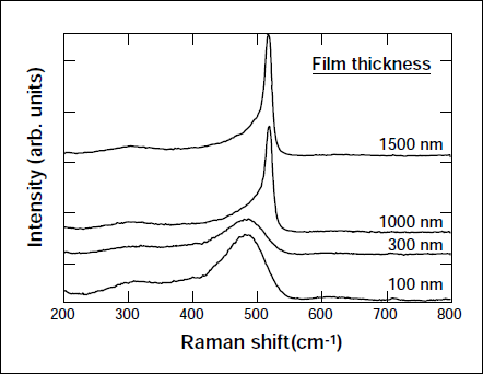
Fig.1 Raman spectra for various Si film thickness after FLA treatment.
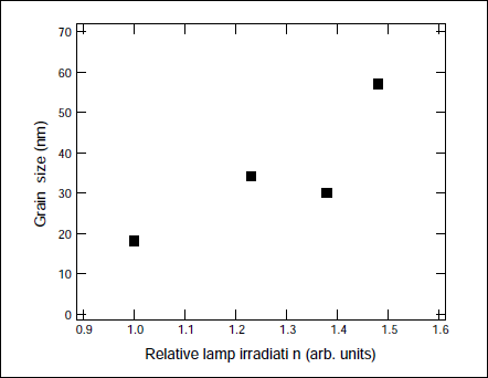
Fig.2 Grain size in crystallized Si films with thickness of 1.5µm as a function of relative lamp irradiance.
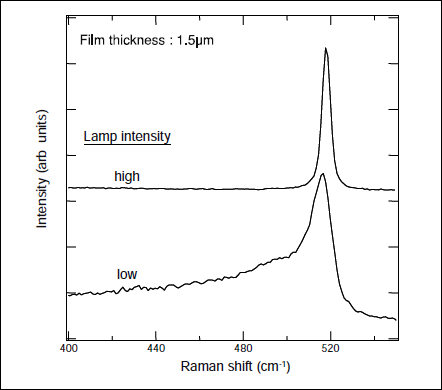
Fig.3 Raman spectra for crystallized Si films with thickness of 1.5 µm treated under various lamp irradiance.
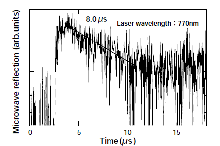
Fig.4 Microwave reflection decay measured by µ-PCD for the ngp-Si film with thickness of 1.5µm after HPWVA treatment.
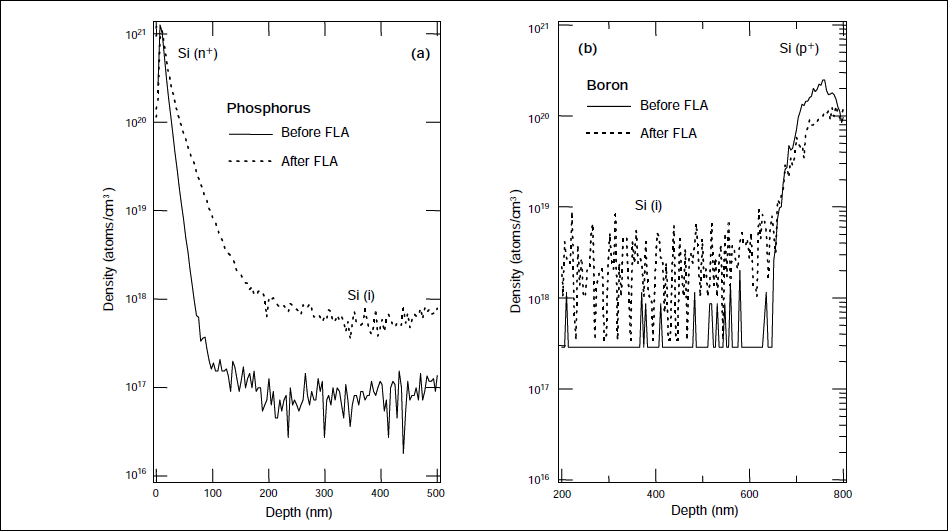
Fig. 5 SIMS profiles for (a) phosphorus and (b) boron atoms before and after FLA.
4. Conclusions
In this study, we clarified that a-Si films formed by Cat-CVD with thickness of over 1.5µm deposited on quartz substrates can be successfully crystallized by FLA. The strongly irradiated films exhibit high crystallinity as well as the grain size of lower than 60 nm, indicating formation of ngp-Si. HPWVA treatment is effective to terminate defects for these ngp-Si films and consequently a long minority carrier lifetime of 5-10µs is observed from the ngp-Si films only after HPWVA. This surprisingly long carrier lifetime corresponds to the minority carrier diffusion length of over 10µm assuming minority carrier mobility of 10cm2/Vs. Dopant diffusion during the FLA treatment is so small that p-i-n structures have been maintained. Therefore, the FLA process and ngp-Si films formed by it are applicable for high-efficient thin film solar cells.
Acknowledgments
This work is supported by New Energy and Industrial Technology Development Organization (NEDO).
関連製品

論文を探す
フラッシュランプを用いた瞬間熱処理技術の関連論文を中心に、2006年に各学会や研究会で発表した論文13件、専門誌への投稿論文4件をご紹介します。
(2007年08月)