光技術情報誌「ライトエッジ」No.35(2011年8月発行)
2010.9 Reprinted by permission from Nature Photonics Vol.4, pp.767-770, November 2010 Copyright: Macmillan Publishers Limited
100 mW deep-ultraviolet emission from
aluminium-nitride-based quantum wells pumped
by an electron beam
Takao Oto1), Ryan G. Banal1), Ken Kataoka2), Mitsuru Funato1)
and Yoichi Kawakami1)★
1) Department of Electronic Science and Engineering, Kyoto University,Kyoto 615-8510, Japan,
2) SSLS Development Department, Ushio Inc., Himeji, Hyogo 671-0224, Japan.
★ e-mail: kawakami@kuee.kyoto-u.ac.jp
Ultraviolet light sources, represented by excimer and mercury lamps, are currently used for various applications, including water purification/sterilization, biotechnology, photolithography and surface modification. However, they have the disadvantages of limited portability, low emission efficiency and the presence of harmful constituents. Finding a compact, efficient and environmentally friendly alternative ultraviolet light source is therefore of considerable technological interest. Aluminium-nitride-based semiconductors show promise as materials for this purpose1‒13, but because of difficulties in controlling electronic conductivity, in light-emitting diodes are hampered by low external quantum efficiencies. Here, we use an electron-beam pumping technique, demonstrating an output of 100 mW and a record power efficiency of ~40% from AlxGa1-xN/AlN quantum wells emitting at ~240 nm. This achievement is attributed to carrier confinement within the high-quality quantum wells, as well as the appropriate design of sample structures for electron-beam pumping, and may be a milestone in the path to realizing next-generation ultraviolet light sources with great ecological and economic benefits.
Aluminium nitride (AlN) and high-aluminium- content AlxGa1-xN/AlN quantum wells have recently been the subject of extensive study1‒13, because AlxGa1-xN has a direct bandgap that can be tuned for the ultraviolet (UV) region between 200 and 300 nm by adjusting the composition of the aluminium. Crystal quality has now been improved dramatically, enabling internal quantum efficiencies (IQEs) at room temperature to reach 70% (see Methods) at a wavelength of 280 nm (ref. 4) and 50% at 250 nm (ref. 5). We have also fabricated high-quality AlxGa1-xN/AlN quantum wells on sapphire (0001) substrates6‒8 that have an IQE of 36% at 240 nm (ref.8). These values are comparable to matured InxGa1-xN/GaN visible emitters14.
A critical factor in electrically driven devices such as light- emitting diodes (LEDs) is the external quantum efficiency (EQE), which is the product of the IQE, carrier injection efficiency (CIE) and light extraction efficiency (LEE). Despite the high IQE that has been achieved, the EQE of AlxGa1-xN-based LEDs is only 3% for emissions between 255 and 280 nm (refs 10,11) and becomes smaller at shorter wavelengths12. Although their reported LEE values are less than 8% (ref. 13), device configurations such as patterned substrates15 may improve the LEE. A more essential factor responsible for a low EQE may be the intrinsically low hole concentrations in p-type AlxGa1-xN. Generally, the wider the bandgap, the deeper the acceptor activation energy becomes; this has been observed in magnesium-doped AlN (630 meV; ref. 1) and GaAs (29 meV; ref. 16). A simple calculation based on Maxwell‒Boltzmann statistics predicts that the hole concentration in AlN with a magnesium acceptor concentration of 1 x 1019 cm-3 is 2 x 1010 cm-3 at room temperature. This very low value degrades the hole-related transport properties.
Several groups have proposed a promising alternative ̶ electronbeam (EB) pumped nitride semiconductor-based light sources ̶ which use a structure similar to a field-emission display. Watanabe and colleagues have fabricated a handheld device using boron nitride powders with an emission wavelength of 225 nm, a maximum output power (Pout) of 1 mW, and a power efficiency (PE) of 0.6% (ref. 17). Additionally, Miyake and colleagues have demonstrated that a silicon-doped AlxGa1-xN bulk-like film excited by EB exhibits an output of 2.2 mW at 247 nm with a PE of 0.22% (ref.18). However, similar to LEDs12,13, their performances are still insufficient for practical applications.
There are two major reasons for this poor performance. The first arises from self-absorption phenomena, in that light-emitting bulks and powders may absorb emitted light, degrading its availability. (In LEDs, the p-type GaN used for improving hole transport properties also absorbs emitted light.) The second reason is that the radiative recombination probabilities in bulks and powders are low compared with quantum wells19. To overcome these issues, we propose using highly luminous quantum wells as a phosphor for EB pumping. In quantum wells, the light-emitting layer has a narrower bandgap than the host material, so absorption by the host material can be avoided in principle. Furthermore, as mentioned above, we have obtained AlxGa1-xN/AlN quantum wells with high IQEs. By virtue of these advantages, we now demonstrate a light output of 100 mW and a PE of ~40% at ~240 nm from AlxGa1-xN/AlN quantum wells pumped by EB.
As illustrated in the inset of Fig. 1, the sample comprised an AlxGa1-xN/AlN eight-period multiple quantum well (MQW) with an aluminium composition x of 0.69, grown on an AlN/sapphire (0001) substrate (see Methods). The AlxGa1-xN well and AlN barrier thicknesses were 1 and 15 nm, respectively, yielding a 128-nm-thick quantum-well region. The reason for the selection of this thin well width is related to the optical anisotropy in AlxGa1-xN/AlN quantum wells9. In thick AlxGa1-xN coherently grown on AlN, the valence band ordering prevents surface emission from the (0001) plane for x > 0.6, that is, for emission wavelengths shorter than 250 nm. In contrast, we have found that the quantum confinement strongly affects the valence band ordering and promotes (0001) surface emission9, which motivated us to use the 1-nm-thick quantum well.
To assess the fundamental optical properties, photoluminescence (PL) measurements were performed at 8.5 K and room temperature (see Methods). Figure 1 shows the acquired PL spectra with an emission wavelength of ~237 nm at room temperature. The PL intensity ratio between room temperature and 8.5 K estimated the IQE at room temperature to be as high as 57%. It is noteworthy that the IQE of an AlN thick film has been estimated to be ~5% at room temperature3. The much higher IQE of our quantum well is due to the carrier confinement within the very high-quality quantum well. Before achieving this value, it was necessary to optimize the formation of the AlN/sapphire interface6 and the crystal growth of AlN and AlxGa1-xN (refs 7,8). Another important finding in Fig. 1 is that emission from AlN is not observed, indicating that carriers generated in the AlN barriers are eventually captured in the AlxGa1-xN wells. Thus, thin AlxGa1-xN wells (1nm) and suffi-ciently thick AlN barriers (15 nm) are desirable in order to suppress self-absorption in the AlxGa1-xN wells and to supply them with as many carriers as possible.
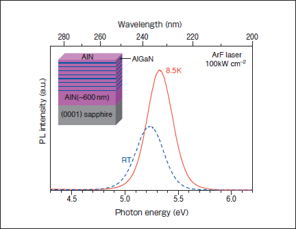
Figure 1 : Fundamental optical properties. The inset is a schematic of an Al0.69Ga0.31N/AlN MQWgrown on AlN (600 nm)/sapphire (0001). PL spectra of Al0.69Ga0.31N/AlN MQW were acquired at 8.5 K and room temperature, from which the IQE was evaluated to be 57%.
Figure 2 schematically depicts the setup of the EB pumping experiments (see Methods). An EB was focused on the sample surface with a diameter of 0.5 mm. The photodetector, a 1 x 1 cm2 AlxGa1-xN photodiode, was placed 3 mm behind the sample to monitor the emission power through the sapphire substrate. To enhance light extraction by avoiding total reflection at the substrate/vacuum interface, the back of the substrate was roughened by a mechanical process. We confirmed that this roughened surface enhanced the light extraction by ~50%.
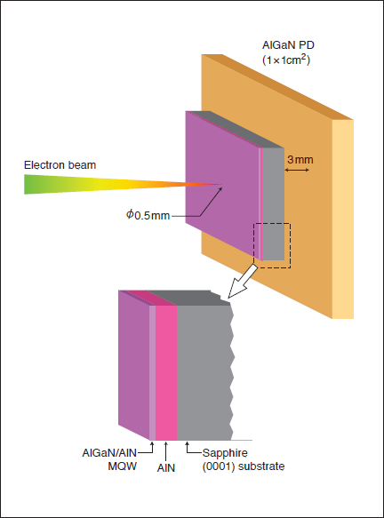
Figure 2 : Schematic configuration of EB pumping experiments. Al0.69Ga0.31N/AlN MQW with a rough back side is irradiated with a focused EB. An AlxGa1-xN photodiode is placed 3 mm behind the sample and monitors the emission power through the substrate.
Figure 3 presents the cathodoluminescence (CL) spectrum of the Al0.69Ga0.31N/AlN MQW and the responsivity of the AlxGa12xN photodiode. The band-edge emissions from AlN and Al0.69Ga0.31N were observed at 210 and 238 nm, respectively. A relatively weak deep-level emission at ~320 nm was due to the AlN/sapphire interface region, which was rich in mismatch dislocations, because that emission was detected though the substrate, but was not from the surface. Because the AlxGa1-xN photodiode was insensitive to light with wavelengths longer than 280 nm, only the emission near the band edge contributed to the estimation of Pout.
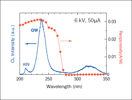
Figure 3 :CLspectrum with photodiode responsivity. CL spectrum of the Al0.69Ga0.31N/AlN MQWand the responsivity of the AlxGa1-xN photodiode measured at room temperature.
Electrons irradiated onto a solid penetrate into the solid and experience mutual interactions with other electrons and atomic nuclei. The penetration depths are generally larger for higher acceleration voltages (VA) and lower-density solids. If the penetration depth is much greater than the thickness of the quantum well region, some of the irradiated electrons may go through that region and recombine in the underlying AlN layer, degrading the CIE. However, if the penetration depth is too narrow, then quantum wells located deeper away from the surface do not receive a sufficient number of carriers. Therefore, to maximize the PE and Pout, appropriately selecting VA to match a given quantum well structure or, conversely, designing a quantum well structure to meet the VA, is crucial. To determine the optimum combination of quantum well structure and VA, we simulated numerous electron trajectories in our MQW under different VA using a Monte Carlo method (software ʻCASINOʼ , available at http://www.gel.usher brooke.ca/casino)20. Figure 4a shows a result for VA=8kV.
For more quantitative analyses, Fig. 4b summarizes the VA dependences of the electron energy absorbed within the quantum well region (left axis) and the rati of that absorbed energy to the energy irradiated onto the sample ( right axis ). The former corresponds to the energy used to generate electron‒hole pairs in the quantum well region, and was maximized at VA=8kV. However, further increasing VA decreased it by the mechanism explained above. Therefore, VA=8 kV should be the best in terms of maximizing Pout. On the other hand, the energy ratio (right axis of Fig. 4b) represents the utilization of irradiated electrons within the quantum well region and corresponds to CIE. Again, VA > 8kV degraded the ratio by the same mechanism. Although the ratio is high for VA < 8kV, the penetration of electrons is insufficient to cover the entire quantum well region. The simulation therefore indicates that a VAbetween 6 and 8 kV is suitable for the current MQW structure.
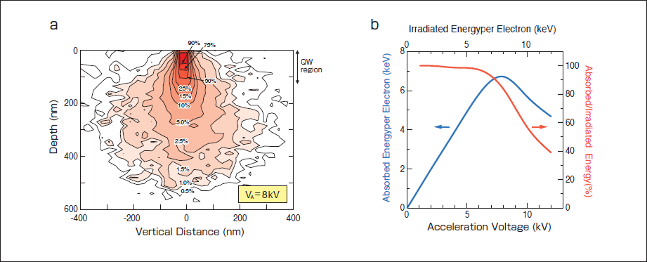
Figure 4 : Electron penetration. a, Contour plot of the electron energy for VA=8 kV simulated by the Monte Carlo method. The assumed structure is an Al0.69Ga0.31N (1 nm)/AlN (15 nm) eight-period MQW. The vertical axis is the depth from the sample surface. Percentages represent the electron energy with respect to the initial value. For example, ʻ90%ʼ means that 10% of the electron energy is absorbed in the solid. b, Summary of the Monte Carlo simulation showing the VA dependence of the absorbed electron energy within the quantum well region (left axis) and the ratio between absorbed energy and irradiated energy onto the sample (right axis).
To confirm the Monte Carlo analysis, Pout was experimentally evaluated using the setup shown in Fig. 2. Figure 5a shows Pout and PE as a function of irradiated current (I). Pout exceeded 100 mW with VA = 8 kV and I = 45µA. However, further increasing VA did not increase Pout, which is consistent with the simulation (Fig. 4b). Furthermore, the PE was also the highest with VA = 8 kV, and was more than 40% for I = 5µA. These experimental results indicated that VA=8 kV is the most suitable VA for our MQW. It is noteworthy that the achieved Pout of 100 mW and PE of 40% are about two orders of magnitude higher than the values reported for LEDs emitting at 250 nm (ref. 12) and EB pumped nitride semiconductors17,18. One discrepancy with the simulation was that VA = 6 kV did not provide a PE comparable to that for VA = 8 kV. A possible reason is the carrier density dependent IQE (unpublished data). Also, the mechanism for the PE drop observed for larger currents has yet to be clarified. These are to be the subjects of future studies.
The efficiencies are discussed, using experimental results of IQE = 57%, an emission energy (E) of 5.2 eV (238nm), and Pout of 100 mW for VA=8 kV and I=45µA. As detailed in the Methods, we consider the relationship PE/ηEH=IQExLEExCIE, where ηEH (0 ≤ ηEH ≤1) is the yield for an irradiated electron to generate electron‒hole pairs in solids. It is difficult to experimentally quantify CIE. Therefore, the value estimated using the Monte Carlo simulation (right axis of Fig. 4b) was used, in other words, 84% for VA = 8 kV. Substituting these quantities into PE /ηEH = IQE x LEE x CIE results in ηEHx LEE = 0.58. For example, LEE = 58% for ηEH = 100%. Although in order to determine these values we have to determine one of them in other experiments, the condition ηEHxLEE = 0.58 seems reasonable, because the emitted light is efficiently extracted from the roughened back of the sapphire substrate.
Figure 5b shows a photograph of a phosphor-coated glass excited by UV emission from our Al0.69Ga0.31N/AlN MQW under the conditions of 8 kV and 45µA. The coated phosphors were identical to those used for fluorescent lamps. In this particular case, the distance between the MQWand the target phosphors was ~15 mm, which is much larger than that between the MQW and photodiode used for Fig. 5a (3 mm). Nevertheless, the phosphors emitted a dazzling white colour, confirming the high Pout from our MQW.
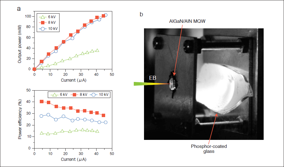
Figure 5 : Electron beam pumping. a, Pout and PE as functions of irradiated current under different VA. Pout in excess of 100 mWis achieved at VA>8 kV and I = 45µA. Maximum PE greater than 40% is obtained at VA= 8 kV and I =5µA. b, Photograph showing a phosphor-coated glass excited by UV emission from our Al0.69Ga0.31N/AlN MQWunder 8 kV and 45µA. All measurements were performed at room temperature.
The present results suggest that the low EQEs of state-of-the-art UV LEDs are not due to low IQEs, but predominantly to low CIEs. However, for EB pumped devices, once high-quality quantum wells have been obtained, significant levels of PE are expected. It should be emphasized that the EB operating conditions in this study (~8 kV and <50mA) are accessible using portable field-emission devices. Additionally, preliminary experiments showed that Pout did not decrease at all over a period of about an hour with VA = 6 kV and I = 35µA. We therefore believe that EB pumping of quantum wells is extremely effective for generating UV light, and the present developments form a significant step towards a nextgeneration, compact, high-efficiency UV light source.
Methods
Estimat ion of IQE. A widely used method with which to experimentally estimate IQE is described. The ratio of the PL integrated intensity at room temperature to that at a low temperature is first evaluated. With an assumption that non-radiative recombination processes can be neglected at low temperatures21, the PL intensity at low temperatures can be regarded as an IQE of 100%. The abovementioned PL intensity ratio can then be used to estimate the IQE at room temperature.
Crystal growth. The growth method was modified migrationenhanced epitaxy (MEE) based on metallorganic vapour phase epitaxy6-8. This method is a hybrid of conventional MEE and a simultaneous source supply, where the latter is inserted into the former. High-quality AlN with a thickness of ~600 nm was initially grown on a sapphire (0001) substrate at 1,200 8C by modified MEE using trimethylaluminium (TMA) and ammonia as source precursors. AlxGa1-xN/AlN MQWs were then fabricated by modified MEE while supplying additional trimethylgallium (TMG) together with the TMA. As well as controlling the thickness of the barrier and well layers on a per-growth-cycle basis (AlN barriers, 21 cycles; AlGaN wells, 1 cycle), this method enabled an atomically flat surface to be maintained. To induce gallium into the quantum wells, the growth temperature was decreased from 1,200 to 1,080 8C. The quantum well parameters, including aluminium composition, well widths and barrier widths, were derived from transmission elect ron microscopy and the satellite peaks observed in X-ray diffraction (XRD) measurements. Reciprocal space mapping by XRD was also performed to confirm the coherent growth of AlxGa1-xN/AlN MQWs with respect to AlN underlying layers.
Optical measurements. The PL measurements were carried out at 8.5 K and room temperature. The excitation source was a pulsed ArF excimer laser ( λ= 193nm, τ= 4ns, 25 Hz and 100kW cm-2). The spectra were acquired using a 30-cm monochromator (resolution, 0.1 nm) in conjunction with a liquid-nitrogen-cooled charge-coupled device camera.
Figure 2 shows the setup for the CL measurements. The sample, EB gun and photodiode were loaded in the same vacuum chamber. EB generated by thermionic emission was accelerated by VA and focused using electromagnetic lenses. The VA varied between 0.1 and 30 kV, and the emission current was varied below 110 µA. The irradiated current was estimated using a Faraday cup adjacent to the sample. The AlxGa1-xN photodiode was produced by ALGAN K.K., Japan, and its responsivity (shown in Fig. 3) was calibrated at the National Metrology Institute of Japan22. Both the sample and the photodiode were mounted on an aluminium block, which served as a heat sink, so that the effects of heat generation by nonradiative processes could be neglected. The luminescence excited by EB (that is, CL) was collected outside the vacuum chamber that held the sample through a viewing window composed of synthetic quartz. The spectra were acquired by the same detecting equipments for the PL measurements.
Definitions of efficiencies for EB pumping. To estimate EQE during EB pumping, it should be noted that one irradiated electron generates multiple electron‒hole pairs in solids. Using the yield (ηEH ) of that process, the number of electron‒hole pairs per irradiated electron is expressed by ηEHVA/E (0 ≤ ηEH ≤ 1), which leads to the EQE definition of (Pout/eE)/((ηEHVA/E)(I/e)). Here, e is the elementary charge. Then, taking PE = Pout/(IVA) and EQE = IQE x LEE x CIE into account, we obtain PE/ηEH = IQE x LEE x CIE.
Received 3 June 2010; accepted 18 August 2010; published online 26 September 2010
論文を探す
次世代の最先端半導体を製造するEUV露光装置用の「光源」をはじめ、LEDやFPD製造分野、医療分野における「光の装置」の研究開発、また、注目を集める「固体光源」に関する研究など、2010年秋から2011年春にかけて発表した論文9件を掲載しました。
また、シリーズ「大学研究室を訪ねて」では、医食同源の実現に向けて、植物と環境を研究ターゲットに、環境調節工学に取り組む千葉大学 大学院園芸学研究科教授の後藤英司先生をご紹介しております。
(2011年08月)