光技術情報誌「ライトエッジ」No.43(2016年04月発行)
ECTC 2015
(2015.05)
Modeling, Design and Fabrication of
Ultra-thin and Low CTE
Organic Interposers at 40µm I/O Pitch
Zihan Wu, Chandrasekharan Nair, Yuya Suzuki, Fuhan Liu, Vanessa Smet, Daniel Foxman*,
H. Mishima*, Furuya Ryuta+, Venky Sundaram, Rao R.Tummala
3D Systems Packaging Research Center Georgia Institute of Technology Atlanta, GA 30332
Mitsubishi Gas Chemical*, Japan
Ushio Inc.,+ Japan
Email: zwu77@gatech.edu
Abstract
This paper presents a comprehensive study on the fundamental factors that impact the scalability of organic interposers to 40μm area array bump pitch, leading to the design and fabrication of ultra-thin and low CTE organic interposers at 40μm pitch. Silicon interposers were the first substrates used for 2.5D integration of logic and memory ICs at close proximity. However, the high cost and electrical loss of wafer back end of line (BEOL) silicon interposers has fueled the need for fine-pitch organic interposers. Organic substrates face two primary challenges in achieving finer I/O pitch: layer-to-layer mis-registration during copper-polymer re-distribution layer (RDL) fabrication due to the thermo-mechanical stability issue of organic laminate cores, and warpage during chip assembly on thin core substrates. This paper studies these two fundamental factors by finite element modeling (FEM) and experimental characterization, resulting in RDL design guidelines for low mis-registration and warpage. Reducing the copper thickness in each layer as well as the thickness of the polymer dielectric to below 10μm, resulted in significant reduction in CTE mismatch- induced stresses at different interfaces. The modeling-based design was verified by fabrication of a multi-layer RDL stack on 100μm thin low coefficient of thermal expansion (CTE) organic cores with ultra-thin build-up layers to achieve a bump pitch of 40μm. The assembly of chips on the thin organic interposer was optimized to minimize the warpage, leading to the demonstration of two-chip 2.5D organic interposers.
Introduction
The thermal and cost challenges of 3D IC stacking have accelerated the development of fine-pitch 2.5D interposers for logic-memory, memory-memory and logic-logic integration with highest bandwidth at lowest power consumption. Although silicon interposers from wafer back end of line (BEOL) processes have been demonstrated with sub-micron re-distribution layers (RDL) for high bandwidth chip-to-chip interconnections [1], they suffer from high cost and high electrical loss. Large panel processing on glass and organic cores offers a compelling lower cost alternative to silicon interposers due to the larger number of unit interposers per panel. Organic laminates are especially important since they leverage existing panel manufacturing infrastructure. Shinko Electric, Japan was the first to demonstrate 40μm I/O pitch organic interposers [2], but used thick cores (400-800μm), and thinfilm wiring processes adopted from wafer processing to fabricate 2μm wiring with 10μm diameter RDL vias on top of chemical-mechanical polished (CMP) build-up organic substrates. Kyocera Japan demonstrated thinner organic cores of 200μm with RDL, but feature sizes were limited to 6μm with RDL via diameters of 20μm on 32μm pads [3]. Samsung Electro Mechanics recently reported on solutions for small feature sized organic interposers, using photo-defined RDL vias and thinfilm processes on one side of organic laminate cores [4]. However, there is a critical need to establish the limits of pitch scaling of organic interposers as a function of core thickness, based on fundamental studies of layer-to-layer mis-registration and warpage of low CTE organic cores. This paper describes the progress in demonstrating a new concept in realizing low-cost and ultra-thin 2.5D organic interposers at 40μm bump pitch, as shown in Fig. 1.
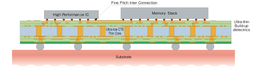
Fig. 1. Concept of ultra-thin low CTE organic interposer
A particular focus of this paper provides fundamental understanding of the factors that limit the pitch scaling of organic interposers, namely, layer-to-layer via mis-registration and warpage. The CTE mismatch between the low CTE organic laminate core and copper-polymer RDL layers induces dimensional instability, thus limiting the precision of via-to-pad registration in forming multiple wiring layers. Finite element modeling (FEM) was conducted by varying the CTE and modulus of laminate core and thickness of polymer and copper to arrive at the optimal stack-up for lowest warpage during multi-chip assembly. The second part of this paper focuses on converting the modeling outcomes into the design and demonstration of organic interposers. The first RDL test vehicle was designed at 40μm pitch with 100μm thick, ultra-low CTE (~ 1.5ppm/℃) laminate core, integrating ultra-thin dry film build-up dielectrics with low cure shrinkage, and thin copper metallization layers to minimize the RDL-induced stresses. The second six-metal layer (2+2+2) test vehicle was designed to quantify assembly-induced warpage with both thermo-compression bonding (TCB) and reflow at 260 ℃ under various conditions. The final section considers the dominant factors limiting the registration and warpage during interposer fabrication and assembly, and proposes a preliminary design rule to fabricate and demonstrate 2.5D organic interposers at 40μm bump pitch.
Fundamental Study of Pitch Scaling Factors
●Preliminary Study on Dimensional Stability
The dimensional instability of laminate cores is one of the major barriers in achieving a high-density 2.5D organic interposer. This dimensional instability occurs due to two primary reasons:
(1) Thermal stability issue of the laminate material
Generally, laminate core materials have a glass transition temperature (Tg) of between 200-230℃ while materials like glass, have a Tg of ~500℃. The substrates are exposed to the highest processing temperatures of 200℃ during RDL dielectric polymer curing and 260℃ during solder reflow cycles for chip- and board- level assembly. In this study, the problem of thermal stability was addressed by choosing high Tg bismaleimide triazine (BT) laminate cores with a Tg of ~ 300℃.
(2) Build-up of residual stresses in the laminate core during the fabrication processes
The dielectric curing temperatures during the RDL fabrication process are close to 200℃. At this temperature, the CTE mismatch between Cu (17 ppm/℃) and the high Tg BT laminate core (~ 1.5 ppm/℃) will lead to an increased build-up of residual stresses in the substrate. Since the laminate core is a viscoelastic material, these residual stresses are compensated in the form of shrinkage of the substrate during the subsequent heat and cool cycles. This leads to a via-pad misalignment in the RDL layers. Reduction of residual stresses during the build-up processes was achieved by using ultra-thin dry film dielectric (~ 5 μm) and Cu (~ 2.5 μm) in the RDL layers. Also, the advanced BT laminate cores used in this study had higher elastic modulus (~ 40 GPa) compared to standard FR4 laminates (10 - 15 GPa). This helped reduce the substrate warpage during the RDL fabrication process.
● Warpage Modeling for Assembly
FEM-based simulations were used to analyze the warpage behavior during multi-chip assembly process. A six-metal layer (2+2+2) ultra-thin low CTE organic interposer was modeled with its schematic diagram shown in Fig. 2. RDLs on double sides had symmetric structures for this modeling and the stack-up details are provided in Table 1.
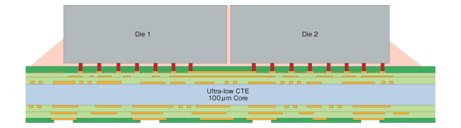
Fig. 2. Design of test vehicle for warpage analysis.
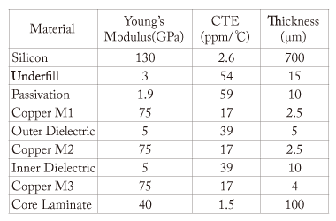
Table 1. Material properties used for low CTE ultra-thin interposer warpage analysis modeling
Interposers with a body size of 19mm × 24mm were assembled with two homogeneous silicon ICs with a size of 10mm × 10mm each. The inner layer on the organic core emulated power and ground planes, while the two outer most metal layers emulated high-density signal routing in terms of the copper distribution. Photo-sensitive polymer passivation layers were assumed to be present on both sides of the substrate for chip- and board-level assembly. A simplified quarter-symmetrical FEM model based on plane-strain approximation was built in ANSYSTM. Since this study focused on the impact of material properties and geometry variations on the warpage behavior of 2.5D organic interposer after first-level chip assembly, a 2D model was built to conduct this study [5]. The RDL structures were simplified in the model, by simulating the irregular copper circuit patterns using an equivalent copper sheet according to its coverage in volume [6]. The warpage behavior was analyzed after 260℃ reflow for dies assembly. The simulation result for warpage behavior is shown in Fig. 3(a). In comparison to the result in Fig. 3(a), two other models were built with modified parameters such as CTE of the core and the thickness of the RDL stack, and these results are shown in Fig. 3(b) and Fig. 3(c). The models used to generate the results shown in Fig. 3(b) used the same stack-up structure but used high CTE 100μm FR-4 as the core laminate. The modeling results shown in Fig. 3(c) doubled the thickness of copper for each metallization layer as well as the RDL dielectrics on high CTE cores. The deformation of vertical direction was scaled by a factor of 15 for easy visual observation of the warpage behavior.
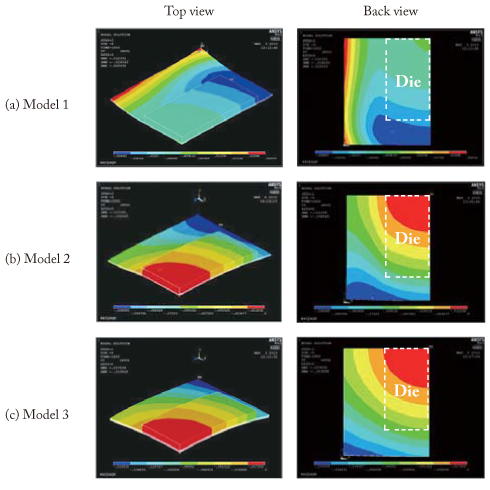
Fig. 3. FEM simulated overall warpage of: (a) 53μm with low CTE core and ultra-thin dielectrics, (b) 107μm with high CTE core and ultra-thin dielectrics, and (c) 154μm with high CTE core and thick dielectrics after first-level assembly.
The simulation results showed a dramatic warpage drop when low CTE laminate cores were used with ultra-thin build-up dielectrics and reduced copper thickness. The warpage reduction was more apparent in the die shadow region since the large die-to-interposer thickness ratio made the warpage behavior dominated by the silicon die. However, since the overall substrate CTE has been lowered by ultra-low CTE laminate core, a large CTE mismatch between substrate and underfill causes an additional stress, which is gradually released along the substrate from the die shadow region. This warpage can be further reduced by an optimal underfill volume control and further miniaturization of the package size. Both theoretical analysis and modeling results showed the potential of achieving fine pitch on low CTE ultra-thin organic interposers. The modeling results were used to arrive at a preliminary stack-up structure and design for fabrication and characterization of test vehicles to verify the modeling outcomes.
Design and Fabrication of RDL Test Vehicle
● RDL Design
The RDL vehicle targeted 3-5μm fine lines on the both 5μm and 10μm dry film build-up dielectrics at 40-80μm bump pitch on ultra-thin low CTE core laminate. The design concept and specifications are shown in Fig. 4 and Table 2.
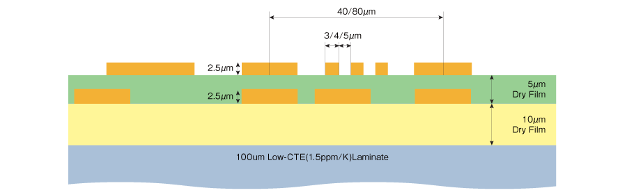
Fig. 4. RDL test vehicle of 2+0+2 stack double-side four-metal layer thin organic interposer.
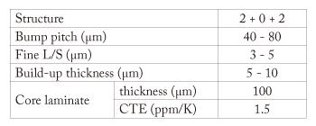
Table 2. Specifications of RDL Test Vehicle
● Fabrication of RDL Test Vehicle
A brief process flow of the RDL test vehicle fabrication is shown in Fig. 5.
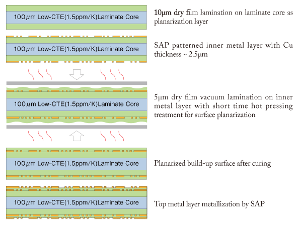
Fig. 5. Fabrication process flow of RDL test vehicle.
In each metal layer design, dummy mesh copper was used to fill up the empty spaces to improve the metal distribution for plating uniformity. The target thickness for the plated copper traces on the internal metal layers was 2.5μm, allowing the 5μm dry film to laminate evenly and achieve good planarity over the copper traces. Advanced semi-additive processes (SAP) and differential spray etching for seed-layer removal were used to metallize the dry film polymers. The overall fabrication results are shown in Fig. 6 and Fig. 7.
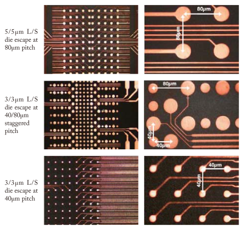
Fig. 6. SAP patterned 3-5μm fine line escape routing on ultra-thin dry films.
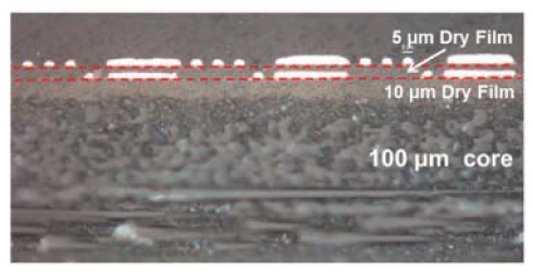
Fig. 7. Cross-sectional view of RDL test vehicle.
No voids were found during the lamination of the 5μm dry films onto the thin inner metal layer, and good surface planarization was achieved on each dry film RDL layer.
Fig. 8 shows the surface roughness (Ra) of the 5μm dry film after chemical desmear. An average value of 38nm was measured by atomic force microscopy (AFM).
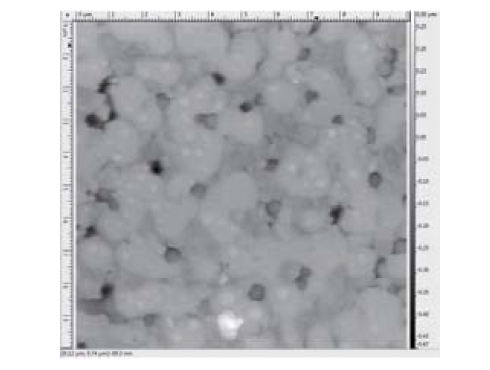
Fig. 8. Surface roughness measurement of the 5μm dry film by AFM.
The fabrication results indicate that the combination of vacuum lamination and hot pressing treatment on ultra-thin dry film build-up dielectrics resulted in a planar surface, suitable for fine line lithography. This process offers a much lower cost approach to ultra-thin multilayer RDL compared to chemical-mechanical polishing (CMP).
Characterization of Layer-to-Layer
Registration and Warpage after Assembly
● Layer-to-layer Registration
The RDL test vehicle was characterized for layer-to-layer mis-registration by high-resolution microscopy. The two-metal layers were automatically aligned using a high-resolution stepper, UX-44101 from Ushio, with an alignment tolerance of ± 1μm. The pad-to-pad mis-registration between RDL layers on a 150mm × 150mm quarter panel was measured as shown below in Fig. 9.
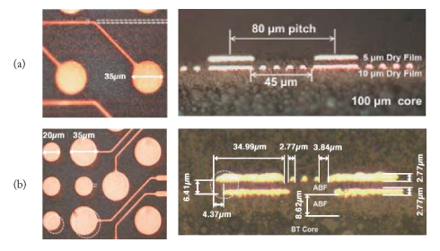
Fig. 9. Mis-registration measurement with: (a) perfect alignment in the center area,and (b) largest measured mis-registration of 4.37μm
The measured mis-registration value indicated that after the curing of the 5μm top dry film dielectric, patterns on the internal metal layer shrunk, which resulted in a maximum of 4.37μm average displacement from their designed locations.
Assembly and Warpage Characterization
A second test vehicle was fabricated with an identical RDL stack to measure the assembly-induced warpage of low CTE ultra-thin organic interposers, and correlate the measured values with the FEM predictions. Both thermo-compression bonding and reflow were used for assembly to verify the temperature and pressure effects on interposer warpage. Three types of assembly were conducted with their conditions listed in Table 3.
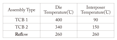
Table 3. Assembly conditions
Warpage was measured from the back side of the interposer, using a Shadow Moiré technique. The measured warpage for the entire interposer before and after assembly was recorded as shown below in Fig. 10. Both attached dies were of 10mm × 10mm in size, with a side by side pacing of 100μm, and package size measured was 19mm × 24mm.
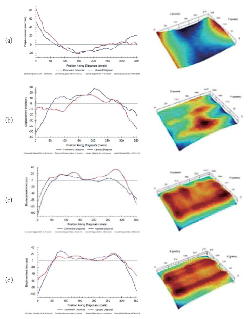
Fig. 10. Warpage measurement in diagonals of the interposers of: (a) +105μm before die attaching, (b) -100μm after TCB 1, (c) -155μm after TCB 2, and (d) -146μm after 260℃ solder reflow
The interposer had an initial warpage of +105μm after the RDL fabrication. For low temperature TCB, the smallest change in overall warpage was found when a low 90℃ heating temperature was applied on the interposer side. Both TCB at a higher interposer temperature of 150℃ and reflow at 260℃, forced the accumulation of a much larger amount of overall warpage. The large CTE mismatch between the high CTE underfill and low CTE interposer forced the interposer edge to warp in an upward direction, once the underfill cooled down from a relatively high curing temperature. The warpage direction of the interposer in the region where dies were attached, was opposite to that of the entire package, shown in Fig. 11.
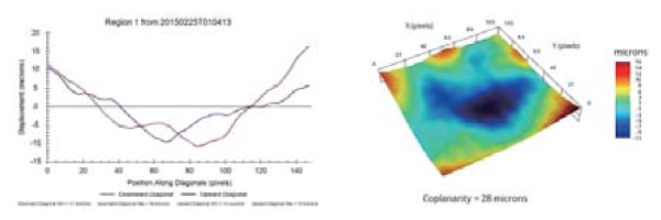
Fig. 11. Warpage of +28μm measured on die 1 shadow region after TCB 2
The warpage results of the die shadow regions under the three different assembly conditions are shown in Table 4.
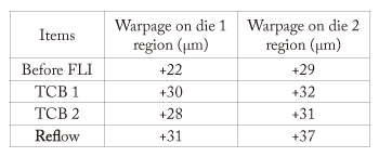
Table 4. Waparge measurement of die shadow regions
The warpage behavior of the die shadow regions was not significant due to the dominant effect of the thick and high modulus silicon dies on the ultra-thin low CTE substrate, which minimized the warpage. In summary, the characterization results verified the warpage trends simulated by finite element modeling. As the interposer core thickness was reduced, both uniformity control during RDL fabrication and assembly have a significant impact on the warpage behavior of the interposer.
Proposed Design Rules for 40 μm Pitch
Ultra-thin Organic Interposer
The modeling and characterization results for mis-registration and warpage, were combined with the feasibility of sub-10μm micro-via formation by excimer laser ablation in thin dry film polymers [7], to arrive at a complete set of design ground rules for 2+2+2 six-metal layer ultra-thin organic interposers at 40μm in-line bump pitch. The proposed design rule cross-section schematic is shown in Fig. 12.
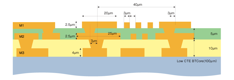
Fig. 12. Proposed design rules for 40μm pitch ultra-thin organic interposer.
The concept of this design rule was to utilize the two topmost layers, M1 and M2, for high-density routing in order to reduce the total layer count. For this stack-up, 5μm was assumed to be the mis-registration value in the worst case scenario for the M2 layer. Considering an existing 2μm misalignment for excimer via ablation location accuracy, 25μm landing pads were designed on M2 to capture 10μm diameter vias, with two 3μm wires escaping out from 40μm pitch bump landing pads. As for the M1 layer, since it does not have to include assembly tolerances, only via mis-location was considered and a 20μm pad size design was proposed so that three 3μm lines can escape through the channel between two adjacent via pads.
Conclusions
In summary, this paper presents a systematic approach based on fundamental limits of organic core materials to demonstrate ultra-thin and low CTE organic interposers at 40μm pitch using panel based double side processes for much lower cost than wafer BEOL silicon interposers. Modeling and measurement were used to quantify two major factors in achieving the goals of 40μm I/O pitch with less than 200μm thick organic interposers, namely, layer-to-layer via mis-registration during RDL fabrication and warpage during assembly. The modeling and characterization of various RDL stacks and organic core properties resulted in the selection of low CTE laminates and ultra-thin copper and polymer dielectric layers for lowest layer-to-layer mis-registration and warpage. A six metal layer interposer design rule was proposed to achieve 40μm I/O pitch routing. This paper describes the progress leading to the first demonstration of low-cost and ultra-thin 2.5D organic interposers at 40μm I/O pitch.
関連製品
論文を探す

1995年の創刊以来、光技術の進展と共にお届けしてまいりましたウシオ技術情報誌「ライトエッジ」が本年、20周年を迎えました。
これを記念をして、今号より誌面のリニューアルを行ないました。
ご好評いただいている弊社技術論文や大学・研究者の方々へのインタビュー「大学研究室を訪ねて」はそのままに、さまざまな業界の著名な方々にご登場いただき、多彩な角度から光にアプロ̶チする「Interview」、そして弊社技術者の取り組みをご紹介する「開発者インタビュー」を新たに設け、より光の魅力をお伝えしてまいります。
(2016年04月)