光技術情報誌「ライトエッジ」No.26(2003年8月発行)
第9回 電子回路世界大会
(2002年10月)
Predominance of Projection Exposure System to
Contact Exposure System for the Manufacture of Printed Wired Board
Masato Sumiya
USHIO Inc.
Yokohama,Japan
Abstract
BGA, CSP, MCM, etc. companies are developed for improving packaging density. Recently, more highly efficient MCP (multi chip package), SiP (system in package), etc. has been developed. Printed wired boards used as the base of such packaging technology are progressing miniaturization and higher density. Manufacturing technologies developed by semiconductor manufacturing has been also applied. Build-up method, which laminates the wiring layers is adopted in many high-density wiring applications. In the field of exposure method in the semiconductor exposure technology, the shift to a step and repeat projection exposure method from a contact exposure method has begun. The step and repeat projection exposure method has the advantage of high alignment accuracy with no mask damage and an auto scaling function. In order to use the projection exposure method more effectively, it is necessary to understand correctly the features of this method, such as control of exposure, focus control, magnification and distortion of projection lens, and the characteristic of the illumination unit. In this report the comparison of the two methods and the latest development of the step and repeat system in USHIO is described.
1. Introduction
Recently, high-density MCP (multi chip package), high-density Sip (system in package), etc. are developed, and PWB used for these bases are increasing in miniaturization and high-density.
Semiconductor-manufacturing technology is being applied for these high-density PWB manufacturing technology. This is also true for semiconductor exposure technology, the exposure system, which dominates the PWB manufacturing process, is starting to shift from contact exposure method to step-and-repeat projection exposure method.
USHIO has developed Step-and-Repeat Exposure System for achieving high resolution, high overlay registration accuracy, and improvement in the yield. "No contact of a mask with a substrate" and "Able to vary projection magnification along with the expansion and contamination of the substrate (auto scaling function)" are the greatest features of this exposure system.
Step-and-Repeat Projection System is effective system in manufacturing PWB of under 30µm minimum line width patterns and below ±20µm overlay registration accuracy demands. Step and Repeat which is non-contact method have improved the product yield due to less or no damage to mask. Such damage to mask was cause by contacting substrate in past.
2. Contact Exposure System and Step-and-Repeat Projection Exposure System
The contact exposure method has been used conventionally as the exposure system for PWB. The extent of the exposure area and low system cost is effective in manufacturing PWB of above 50µm minimum line width patterns and ±30µm overlay registration accuracy demand level.
However , in recent years, the progress of miniaturiza tion and higher density and higher performance made PWB has evolved with the development of a high-density packages and the manufacturing of high-density PWB such as 20µm minimum line width patterns and below ±15µm overlay registration accuracy demands are being required.In this case, mainly three following problems arise by contact exposure system.
- (1) Due to miniaturization, uniform pattern formation of the whole exposure area surface is difficult. (It is difficult to contact the whole exposure area surface uniformly.)
- (2) The effect of the mask damage and transcription of particle originated by the contact of a mask and a substrate reduces the yield.
- (3) There is a limit to the improvement in overlay registration accuracy due to the expansion or shrinkage of a substrate.
Step-and-repeat projection exposure system can solve these problems.
Table 1 is the comparison of contact exposure system and Step-and-repeat projection exposure system. Stepand-repeat projection system for semiconductors is also indicated as a reference.
Step-and-repeat projection exposure system is inferior to contact exposure system in exposure area and system cost, but shows a great increased performance in the yield and in overlay registration accuracy. This is the result of accommodating the substrate expansion or shrinkage by adopting an auto scaling function and a projection optical system having deep DOF plus no mask damage. It is possible to solve the problems of a contact exposure system.
Recently, processing a substrate by step-and-repeat method has replacing contact exposure system in aim of improving overlay registration accuracy. This means that responding to substrate expansion or shrinkage is required in manufacturing a high-density PWB. According to the necessity for step-and-repeat processing, the difference in the exposure area of a contact exposure system and a step-and-repeat projection exposure system is decreasing substantially.
In Step-and-Repeat projection system, the greatest difference between for the PWB and for semiconductors is the performance of the projection lens installed. As for a projection lens, the exposure area and resolution are in inverse proportion
Although, pursuance of minituauzation in step-andrepeat projection exposure system for semiconductors have yield very high resolution performance, but small exposure area. Moreover, DOF for securing a resolution performance is 1-2µm or less. An also required for high precision, will result in very expensive system.
With consideration of productivity, the step-and-repeat projection system for PWB, projection lens is required to have the balance exposure area and the resolution performance. Furthermore, 50 -100µm DOF need to be secured, corresponds to the printed circuit board that curves greater in compared with a wafer. Also, the large auto scale range of ±1000 ppm is a plus feature for printed circuit boards.
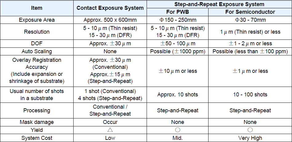
Table 1 - Comparison of contact exposure system and Step-and-Repeat projection system
3. Features of Step-and-Repeat Projection Exposure System
The feature of a step-and-repeat projection exposure system is explained in more detail below.
3-1. Optics
Fig.1 shows the optical system of the projection exposure method. Constructed from two parts, from lamp to a condenser lens is illumination optical system, and from a mask to substrate is a projection optical system. The configuration of illumination optical system of contact exposure method and projection exposure method are about the same.
Please note that mask do no contact substrate. The mask image on to the substrate by projection lens. This projection lens varies by wavelength, exposure area, and resolution. Lens model is mainly determined by the minimum line width pattern demands. Table 2 is the list of USHIO's main Projection Lenses.
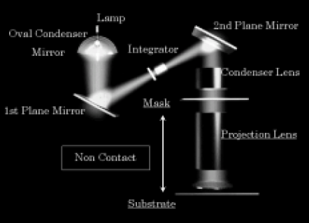
Figure 1 - Optical System Diagram
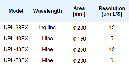
Table 2 - Projection Lens Products
3-2. Contrast of Image
The resolution of the exposure system is determined by the contrast of image formed on a substrate. The appearance of image formed on a substrate both by a projection exposure and contact exposure are shown in Fig.2. The relation between the focus (gap) and resolution is in Fig.3. Fig.2 is a schematic diagram (basic concept) and Fig.3 is the result of a simulation.
Typically, contrast of the image formed on substrate is the maximum value when a mask and a substrate contact completely. That means, the state of perfect contact exposure is the highest contrast and as a result, shows high resolution. However, in most of the contact exposure, it is exposed in the state with some gaps, because of the warp or undulation of a substrate or to avoid the mask damage. The protection film of the photoresist of a substrate may be equivalent to gap. When there is a gap between a mask and a substrate (state of proximity exposure),the contrast of an image falls in proportion to the increase in a gap and the resolution will worse.
On the other hand, even with the zero focus function of the projection exposure (for PWB), contrast equivalent to the state of a complete contact exposure cannot be achieved. This is affected by the resolution of the projection lens. Contrast falls by aberration of a projection lens. The characteristic point is that the change of this contrast (=resolution) is gentle slope compared to the focus position of a projection lens. Thus the deep depth of focus is achieved in projection exposure. Fig. 4 is the exposure result of Dry Film Resist with DOF ±50µm. This is a good resolution performance in this focus range.
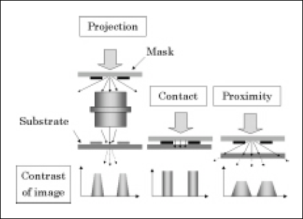
Figure 2 - contrast of image
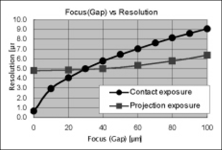
Figure 3 - Focus (Gap) vs Resolution
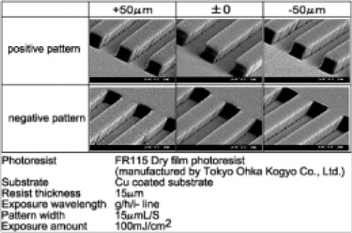
Figure 4 - Dry Film Resist Pattern Profile
3-3. Auto Scale Function and Overlay Registration Accuracy
The substrate expansion or shrinkage of PWB occurs during the process. The expansion or shrinkage could be as much as 250-500ppm. This amount of expansion or shrinkage varies not only by lot but also within the lot as much as up to 200ppm. Furthermore, amount of the expansion or shrinkage varies even with the same substrate surface, and the correction of the expansion or shrinkage with using various mask cannot expect to achieve high overlay registration accuracy. "Function such as able to vary projection magnification along with the substrate expansion or shrinkage (auto scale function)", is the solution to substrate this problem is the biggest feature of projection exposure system. Projection magnification is optimized through the measuring the pitch of actual alignment mark on a substrate and compare to the mask mark pitch.
USHIO actually exposed the sample substrate and evaluated the overlay registration accuracy of the whole substrate surface. The evaluation results using 510x340mm substrate and "Conventional contact exposure system" and "Step-and-Repeat Projection Exposure System (Lens:UPL-38EX)" is Fig.5 notes.
Fig.5 is the evaluation result of overlay registration. The graph shows scattered relative misalignment in X, Y direction of second layer of hole pattern for solder mask to the first layer of land pattern. To compare the first and second layers were each processed by 1) "Contact exposure and contact exposure", 2) "Contact exposure and Step-and-repeat projection exposure", and 3) "Step-and-repeat projection exposure and step-andrepeat projection exposure", See compared accuracy under these three conditions. Consequently, to the overlay registration resulted ±45µm (3sigma) by "Contact exposure and contact exposure", it achieved ±4.3µm (3sigma) by "step-and-repeat projection exposure and step-and-repeat projection exposure" Although there is a difference in substrate size, as was expected, the dramatic effect of an auto scaling function is the key factor.
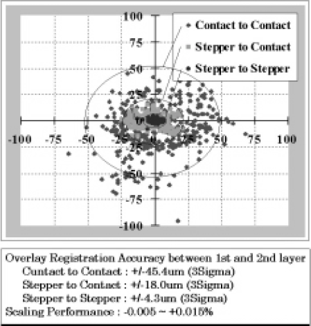
Figure 5 - Alignment Evaluation Data
4.Conclusion
Above mentioned were the introductions to the features of Step-and-Repeat projection exposure system.
It is expected by the characteristic of "No contact of mask with substrate" and "Able to vary projection magnification along with the substrate expansion or shrinkage (auto scale function)" as a leverage, many step-andrepeat projection exposure system will be utilized in manufacturing of a high-density PWB of below 30µm of maximum line width pattern and below ±20µm overlay registration demands.
Selecting the projection lens suitable for each application and taking advantage of this high overlay registration accuracy, more sophisticated and high performance package module PWB is expected to be in production within few years.
関連製品
論文を探す
2002年末に発表し、大きな反響を呼んだ半導体先端パッケージ用ステッパ「UX-7」など露光装置関連に加え、医療分野の投稿、学会発表などをご紹介します。
(2003年08月)