光技術情報誌「ライトエッジ」No.35(2011年8月発行)
2011.3 SPIE Advanced Lithography 2011
Tin LDP Source Collector Module (SoCoMo)
ready for integration into Beta scanner
Masaki Yoshioka1), Yusuke Teramoto2), Jeroen Jonkers1),
Max C. Schümann1), Rolf Apetz1), Volker Kilian1), Marc Corthout1)
1 ) XTREME technologies GmbH, Steinbachstr. 15, 52074 Aachen, Germany
2 ) Gotemba R&D Center, Extreme Ultraviolet Lithography System Development Association (EUVA),
1-90, Komakado, Gotemba, Shizuoka-prefecture, 412-0038, Japan
ABSTRACT
As the traditional techniques used in optical photolithography at 193 nm are running out of steam and are becoming prohibitively expensive, a new cost-effective, high power EUV (extreme ultra-violet) light source is needed to enable high volume manufacturing (HVM) of ever shrinking semiconductor devices. XTREME technologies GmbH and EUVA have jointly developed tin based LDP (Laser assisted Discharge Plasma) source systems during the last two years for the integration of such sources into scanners of the latest and future generations. The goals of the consortium are 1) to solve the wavelength gap - the growing gap between the printed critical dimensions (CD) driven by Moore's Law and the printing capability of lithographic exposure tools constrained by the wavelength of the light source - and 2) to enable the timely availability of EUV light sources for high volume manufacturing.
A first Beta EUV Source Collector Module (SoCoMo) containing a tin based laser assisted discharge plasma source is in operation at XTREME technologies since September 2009. Alongside the power increase, the main focus of work emphasizes on the improvement of uptime and reliability of the system leveraging years of experience with the Alpha sources. Over the past period, a cumulated EUV dose of several hundreds of Mega Joules of EUV light has been generated at the intermediate focus, capable to expose more than a hundred thousand wafers with the right dose stability to create well-yielding transistors. During the last months, the entire system achieved an uptime - calculated according to the SEMI standards - of up to 80%. This new SoCoMo has been successfully integrated and tested with a pre-production scanner and is now ready for first wafer exposures at a customer's site. In this paper we will emphasize what our innovative concept is against old type of Xe DPP and we will present the recent status of this system like power level, uptime and lifetime of components as well.
In the second part of the paper the EUV source developments for the HVM phase are described. The basic engineering challenges are thermal scaling of the source and debris mitigation. Feasibility of the performance can be demonstrated by experimental results after the implementation into the beta system. The feasibility of further efficiency improvement, required for the HVM phase, will also be shown. The objectives of the HVM roadmap will be achieved through evolutionary steps from the current Beta products.
Keywords: EUV sources, gas discharge produced plasma, Tin, EUV lithography
1. INTRODUCTION
EUV sources with high power performance are under development since more than 10 years. Mainly three technologies were investigated, the laser produced plasmas (LPP), the discharge produced plasmas (DPP) and the laser assisted discharge plasma (LDP).
In the LPP sources the plasma is generated by a pulsed, focused laser beam, which hits an appropriate target material. The target mostly used is mass limited in droplet shape to avoid the generation of a large amount of debris. The big advantage of this technology is the scalability of the output power by increasing the laser power. Due to the complex target technology combined with high power laser technology, these sources are however very unstable in terms of pulse to pulse and dose stabilities, because of the limited laser beam stability, the large droplet dimensional, temporal and positional uncertainties and the difficulty to track and synchronize droplets with laser pulses. From a process point of view, dose instability translates into a poor CD uniformity resulting in loss of yield.
Constrained by the ability to sustain stable long burst operations, LPP also exhibits a limited duty cycle, forcing the scanner to wait for the source and detrimentally impacting the effective throughput of the exposure tool.
Finally, because of its proximity to the plasma and exposure to high dose of ions, neutrals, electrons and debris, the collector mirror ‒ the main mirror collecting EUV photons and focusing them towards the scanner ‒ rapidly degrades exhibiting a significant loss of reflectivity and far field uniformity. Despite the efforts at mitigating the degradation of the collector mirror, lifetimes for such very high precision multi-layer optics have yet to exceed few days of continuous operation. The long downtime associated with the necessary replacement of the collector mirror results in a significant Cost of Downtime, dwarfing the very cost of replacement itself (Cost of Consumable). As such, the collector mirror is one of the primary component of the COO in an LPP architecture.
In the DPP sources the plasma is generated within an electrode system by an electrical discharge in the gas phase. The scalability of this technology to higher repetition rates seems limited by the decay of the plasma. In addition to this, higher electrical input power leads to a higher thermal load on the electrodes. Cooling of the electrodes is limited by surface size. On the other hand, DPP demonstrates high stability and achieves a high reliability.
Since 2003 XTREME technologies has been developing laser assisted discharge plasma (LDP) based on tin as a fuel.1,2,3. This hybrid technology combines the main advantages of the traditional LPP and DPP concepts, namely power scalability and high stability. Additional advantages of LDP are:
- ・pure photons, i.e. no tin contamination beyond the scanner interface4 and thus guaranteeing a long scanner life-time
- ・clean photons, i.e. negligible DUV and IR spectral content, enabling imaging and overlay
- ・dose stability and repeatability enabling CD uniformity
- ・high duty cycles enabling throughput, see Figure 1
- ・source uptime enabling the start of massmanufacturing
In this paper we present the present status of LDP technology and future developments.
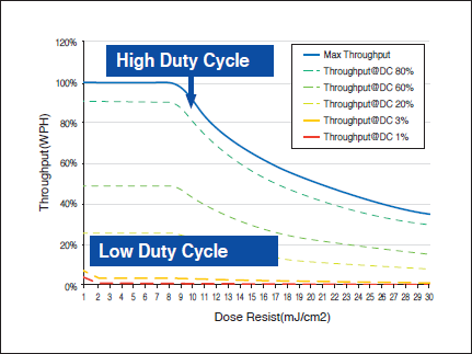
Figure 1: The impact of the source duty cycle upon scanner throughput
2. THE LASER DISCHARGE PLASMA TECHNOLOGY
In LDP the plasma is generated between two rotating discs, see Figure 2. Partially immersed in baths filled with liquid tin, the discs are wetted and covered with a thin layer of liquid tin. A pulsed laser beam focused on one of the discs evaporates a small amount of tin and generates a tin cloud between the two discs. Next a capacitor bank, which is connected to the discs via the liquid tin, discharges and converts the tin cloud into a plasma. Pinched by the high current the plasma emits the EUV radiation. This process is repeated several thousand times per second. The resulting heat-load is cooled away by the liquid tin, which is kept at constant temperature by an external cooler.
To focus the produced EUV light into the scanner, a grazing incidence collector mirror5 is used, see Figure 3. Because all tin plasmas generate tin debris in the form of droplets, clusters, neutrals and ions, it is critical to protect the highly sensitive EUV optics.
XTREME technologies uses a Foil-Trap in combination with an inert buffer gas. Due to collisions with the gas, the tin is redirected to the foils. In a previous contribution1, we showed that this solution enables a very long collector lifetime, leading to a high uptime and a low Cost of Ownership. To prevent tin contamination towards the scanner, baffles are installed between the collector and the wall of the vacuum chamber, see Figure 3. In a separate paper4 it is shown that no tin is found after the IF.
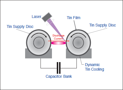
Figure 2 : The principle of the LDP EUV source
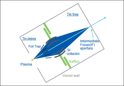
Figure 3 : The collector module transporting the EUV from plasma into the scanner
3. PRE-PRODUCTION SOURCE COLLECTOR MODULE
In 2009 a demons t rator sys tem has been integrated, which is shown in Figure 4. The first results have been reported in reference 6. This source was used for technology development internally at XTREME, producing an EUV dose of more than 20 MJ, equivalent to more than 5000 wafers (assuming 4 kJ per wafer).
Since 2009 this demonstrator has enabled development of technology for the NXE:3100 product source, for instance the cleanliness after IF4 , dose stability and output power at 100% duty cycle. At the demonstrator we achieved 15 W after the intermediate focus, see Figure 5. For further work on power scaling we refer to another paper presented in this conference7.
Figure 6 shows a typical result of the dose stability of LDP. In this specific case a sensor was placed after the Intermediate Focus and the measured EUV energy was fed back into the dose control module. In this way a dose repeatability of 0.09% (3 sigma) was obtained. The dose stability was less than the specified +/- 0.2% over all pulses.
Over the past year XTREME technologies has focused on manufacturing a product source for ASMLʼ s NXE 3100 scanner, integrating the many technologies behind these developments. This source was successfully integrated into scanner8 and shipped to Imec. Figure 7 depicts XTREME source attached to the scanner in the ASML clean-room during system qualification. A movie of the installation of ASML scanner and XTREME technologies EUV light source is available at http://www.youtube.com/imecnanotube#p/a/u/1/2iUPRCMQCGU.
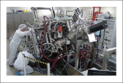
Figure 4: The SoCoMo demonstrator
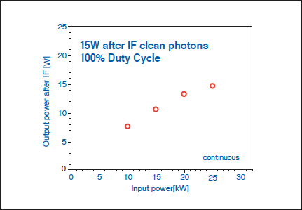
Figure 5: Output power after the intermediate focus (IF) as measured on the demonstrator at 100% duty cycle operation.
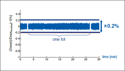
Figure 6: Measured integrated dose stability during simulated scanner operation. In this example a real exposure scenario was simulated over 30 minutes.
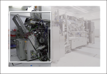
Figure 7: XTREME’s SoCoMo integrated into ASML’s NXE: 3100 scanner (courtesy ASML).
4. HIGH VOLUME MANUFACTURING DEVELOPMENT
To achieve a Cost of Ownership (CoO) making EUV lithography viable in a high volume manufacturing (HVM) environment, the footprint of the scanners needs to be minimized in order to save expensive clean room space. This requires a compact design of the optical system as well as the EUV source itself. A new architecture of the source exhibiting a smaller footprint and leveraging a scaled up version of the existing and proven technology is now being designed (Figure 8).
This new design has a reduced volume, a new beam direction, an increased cooling capability which enables the required higher output power. Whereas the output power of the pre-production system (NXE 3100) will achieve the 100W power level, the output power for the HVM scanners (NXE 3300 series) still needs improvement to reach the required 250W and beyond. This will be achieved not only by raising the electrical input energy per pulse (Figure 9) but also by increasing the repetition rate of the laser. For the latter a value of 40kHz has been demonstrated successfully (Figure 10).
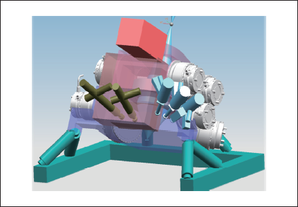
Figure 8 : HVM source model using the proven technology of the beta source in a more compact design
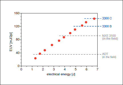
Figure 9: Linear dependence of the output energy per pulse in dependence on the electrical pulse input energy for the different source generations alpha demo tool (ADT), pre-production (NXE 3100) and HVM (NXE 3300 series)
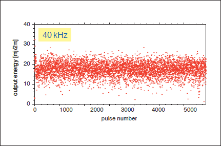
Figure 10: Demonstration of a repetition rate of 40 kHz. The pulse to pulse output energy remains sufficiently constant for the used un-stabilized mode.
5. PRODUCTION RAMP UP
With 24 sources installed worldwide, more than 7000 wafers exposed with ADT and more than 450 wafers equivalent exposed at ASML on NXE 3100, XTREME technologies has enabled the development of EUV.
The experience gained over the years has also positioned the company first on the learning curve: the technology concept is sound and the technology itself has been proven. Because of the high costs involved at EUV, the semiconductor industry cannot afford the design of the source to be stabilized in the field and finalized only several years after its original introduction as it used to being the case at DUV. The design of XTREMEʼ s HVM sources is now being finalized with the goal to reach sufficient maturity at the time of its first introduction
Further beyond, with the final acquisition in 2010 of Philips Extreme UV assets, the Ushio Group ‒ to which XTREME belongs to ‒ has sealed its commitment to EUV lithography and to the semiconductor industry. Leveraging Ushio Groupʼs existing worldwide infrastructure, XTREMEʼs support organization is now being developed and is rapidlymaturing.
Also in 2010, XTREME technologies has leased the premises of the former Mitsubishi semiconductor Fab in Alsdorf, Germany. Located merely 15 kilometers apart from XTREMEʼ s current development facilities based Aachen, Germany (Figure 11, Figure 12), the new building has allowed the company to double the clean room and office space. In 2011, with the lease of the second half of the Fab, the HVM source production will be launched.
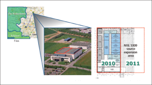
Figure11 : The new facility of XTREME technologies in Alsdorf near Aachen, Germany
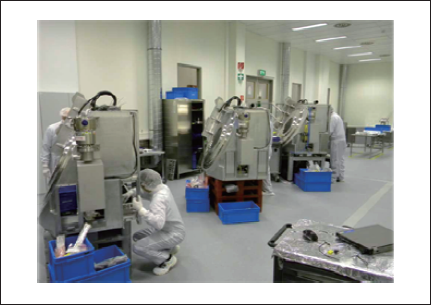
Figure 12: View into the new production facility with three sources under assembly in parallel.
SUMMARY
Joint development activities from XTREME technologies and EUVA led to signific ant performance improvements of tin discharge based EUV sources for pre-production (Beta) scanners during the last year. XTREMEʼs Laser-assisted Discharge Plasma (LDP) technology allows for the combination of scalability, stability, and reliability. The next source generation for HVM scanners is currently in the design phase and a first source of this kind will be assembled within the current year.
ACKNOWLEDGEMENTS
We gratefully acknowledge the contributions of our teams at XTREME technologies and EUVA. Thanks also for their contributions to our development partners ASML, Fraunhofer ILT, Nikon, Media Lar io Technologies, USHIO and Zeiss.
The work performed at XTREME technologies GmbH has been partially funded by the German BMBF under contracts 13N8865 and 13N8866 and by the European Commission within the project “more Moore”. The current development is integrated into the European CATRENE project “EXEPT”. Part of the work is supported by EUVA, Japan.
関連製品
論文を探す
次世代の最先端半導体を製造するEUV露光装置用の「光源」をはじめ、LEDやFPD製造分野、医療分野における「光の装置」の研究開発、また、注目を集める「固体光源」に関する研究など、2010年秋から2011年春にかけて発表した論文9件を掲載しました。
また、シリーズ「大学研究室を訪ねて」では、医食同源の実現に向けて、植物と環境を研究ターゲットに、環境調節工学に取り組む千葉大学 大学院園芸学研究科教授の後藤英司先生をご紹介しております。
(2011年08月)