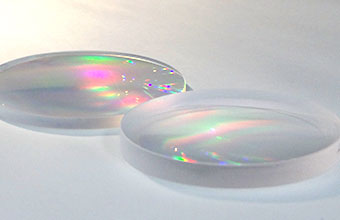
Interference Lithography Technology for exposing periodic submicron patterns seamlessly, using the contrast generatede by light interference
Interference Lithography Technology for exposing periodic submicron patterns seamlessly, using the contrast generatede by light interference
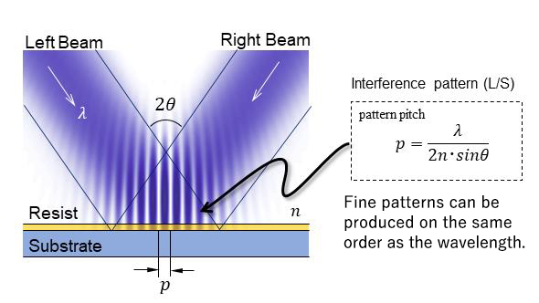
Interference of two coherent lights on overlaid area produces a periodic pattern.
The periodic photo intensity is exposed to the photo resist. Fabricated pattern period is affected by the crossing beam angle, and fine patterns can be produced on the same order as the wavelength. Our laser interference lithography can create high visibility interference fringe by accurate wavefront.
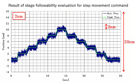
Our high precision work stage realizes fine interference lithography.
The right figure shows result of stage followability evaluation for step movement command. Actual position accurately matches the command position.
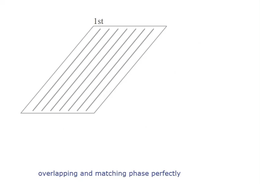
Scanning overlapped phase interference lithography method is a new technology. As the first step, a spot fringe pattern generated by two-beam interference is scanned direction along the grid on the wafer. As the second step, the spot is moved just the integer multiple length of its fringe period, then the spot is exposed again over the 1st fringe pattern. The reason moving amount of spot pattern must be the integer multiple length is to match fringe phases between 1st and 2nd scan perfectly to obtain high contrast exposure.
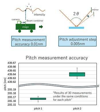
By combining direct measurement technology of interference fringes with precise stage control, we achieve interference fringe pitch measurements with an accuracy on the order of 0.01 nm.
Furthermore, the system is equipped with a compensation optical system that corrects deviations from the target pitch, enabling the high pitch accuracy required for DFB lasers.
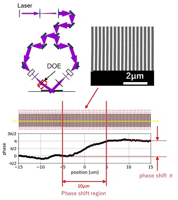
In addition to conventional diffraction gratings, our system supports diffraction gratings with phase-shift structures.
By combining an interference lithography system with DOE (Diffractive Optical Elements), we can fabricate CPM* phase-shift structures.
Unlike the commonly used λ/4 phase-shift structures for DFB lasers, CPM phase-shift structures feature several tens of micrometers wide phase-shift regions. This prevents the concentration of optical intensity, making them suitable for high-power laser applications.
* corrugation pitch modulation
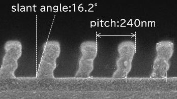
Slanted structure can be created by tilting the optical system.
Free and stable system allow to perfom a variety of evaluation.
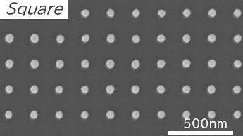
Dot patterns can also be created by precisely performing two exposures with roated angle of the wafer.
we can made square or hexagonal array array by changing the rotation angle of the wafer.
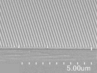
UV laser and stable system can fabricate sub-micrometer pitch patterning.
The SEM image shows 180nm pitch of patterning by interference lithography. It is able to support period up to 150nm.
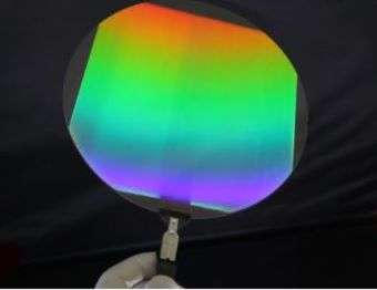
Scanning overlapped phase interference lithography realizes a seamless pattern without stitching caused by Step & Repeat exposure on an entire 8-inch substrate.
In terms of the depth of focus(DOF), patterning is possible on the order of mm. It enables to process that exceeds the restrictions of flatness and flatness.