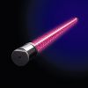
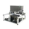
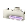
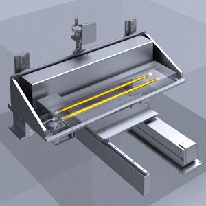
Flash lamp annealer

Flash lamp annealer
  • Modification and Decomposition
  • MEMS, Electronic Components
  • Semiconductors
  • Liquid Crystal Display
  • Printed Circuit Board and PKG

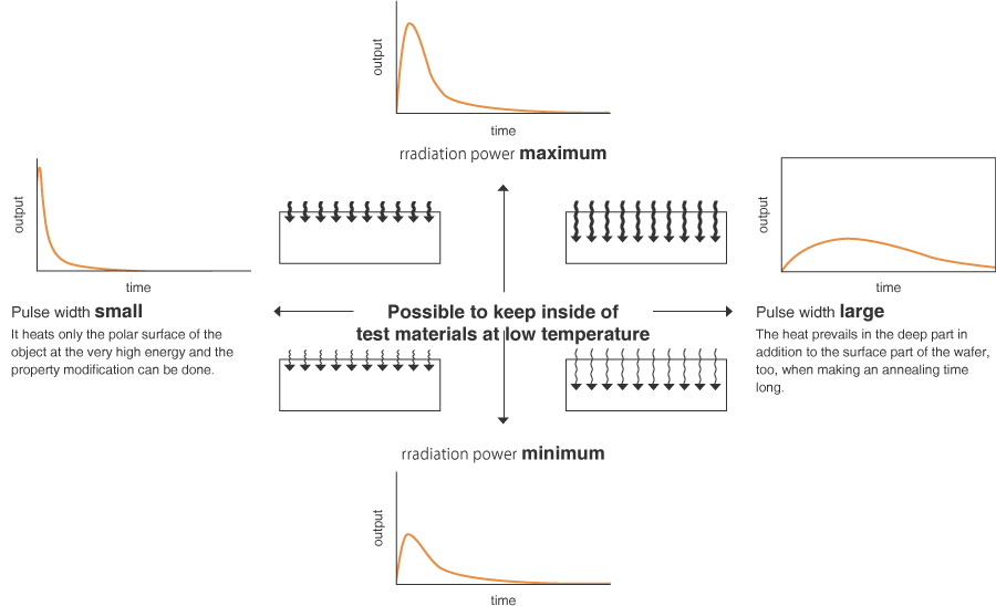
Flash lamp annealing allows very short heating processes as quick as one millisecond.
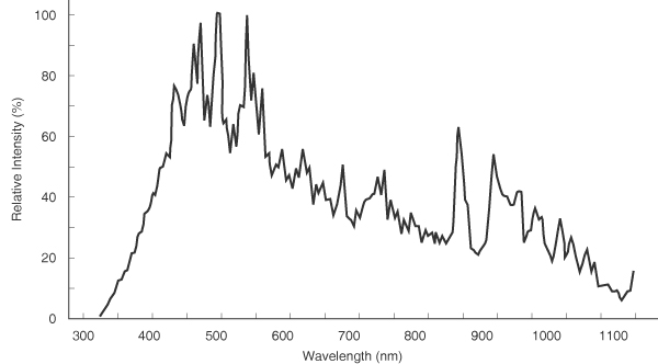
UV to visible wavelength light emitted from the flash lamp can concentrate heat on a substrate (material) surface so that the thermal influence on the underlying film or substrate
can be extremely small compared with conventional heat sources.
This millisecond surface heat treatment is becoming an essential technology for future device developments such as zero diffusion of semiconductor implanted layers and thermal budget reduction.
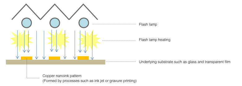
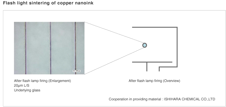
Flash lamp heating is also used to produce reactions such as crystallization, bonding, peeling, decomposition and curing. These characteristics are effectively applied in various research and development applications such as Si wafers, SiC wafers, glass, plastic films and other flexible substrates, as well as in production (manufacturing) line applications.
We welcome requests for experimental demonstrations. Please feel free to contact us.

The ultimate in momentary, zero-diffusion annealing technology within milliseconds
Achieves activation with zero-diffusion Xj control for developing devices beyond the 32 nm design rule by rapid momentary heating.
Process depth control by pulse width management
Managing pulse width controls heating depth and minimizes heat damage to the substrate by heating only the surface layer.
Large-area batch irradiation
High-throughput batch irradiation of large-area substrates has become possible.
High efficiency / Energy saving
Flash lamp wavelength matches the absorption characteristics of Si, so it can be efficiently heated.
Spectrum Example
Process depth control by flash lamp pulse width management
Ultra-shallow junction layer formation
Silicide formation
Ultra-thin oxide film formation
Ferroelectric capacitor deposition
Amorphous silicon polycrystallization
Firing and sintering of metal nano-inks and nano-pastes (e.g., copper)
Si and SiC substrate activation annealing
SOI and SOS substrate annealing
Flexible substrate surface heating
Heating of UV curing and thermosetting resins
and more
Sintering of Cu nanoink light by flash lamp
Conductive Cu nanoink which is sintered at a specific high temperature following pattern formation is attracting attention for use in next-generation printable electronics wiring. By selectively heating just the conductive layer by flash lamp during the heating process, the effect of heat can be minimized even for substrates with low heat resistance and firing can be accomplished in very short times.

Installed light source

How do flash lamps differ from other heat sources?

Whereas other heat sources heat the target object in its entirety, a flash lamp produces only an extremely brief pulse of light that makes it possible to selectively heat just the surface of the target. The ability to heat selectively is useful when heating objects that have low heat resistance, or when the reaction induced by heating is to be limited to just the surface layer of a substrate.