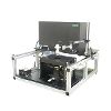
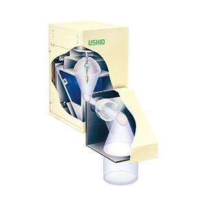
Multipurpose exposure unit Deep UV Multilight
- Litho-Patterning
- MEMS, Electronic Components
- Semiconductors
- Liquid Crystal Display
- Printed Circuit Board and PKG
The Deep UV Multi-light is a light source unit optimized for the deep UV wavelength region from 230 to 330 nm while maintaining the same basic structure of the Multi-light series that has a good track record as a uniform, collimated light source.
It can be applied as a surface modification light source, as a light source for evaluation of various photochemical reactions, as well as for lithographic applications.
Uniform, collimated light source
The optical basic performance is also applicable for adoption in lithography
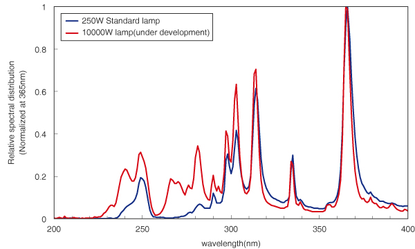
Wideband wavelengths
Encompasses the 230 nm to 330 nm short wavelength region to the typical UV bright line spectrum, such as 365 nm, 405 nm and 436 nm.
Compact, tabletop-size design
Product sizes available for desktop research and development applications to lithography equipment for mass production.
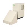
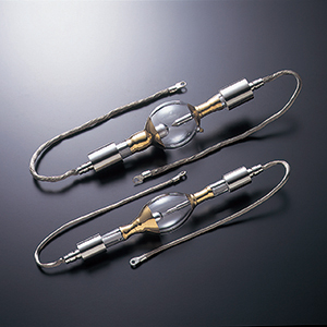
High-intensity short-arc UV light source
Equipped with Ushio's high-intensity short-arc UV lamp, which is best suited for uniform collimated light. Fine patterning achieved.
High illuminance, large-area support
Using the design and manufacture achievements for lithography light source units for Si wafer mass production and large LCD color filter exposure light source units, has enabled a lamp house design aimed at expanding the exposure area and increasing the exposure surface irradiance intensity.
Please consult with us for light source variations up to 10 kW.
Please consult with us for light source variations up to 10 kW.
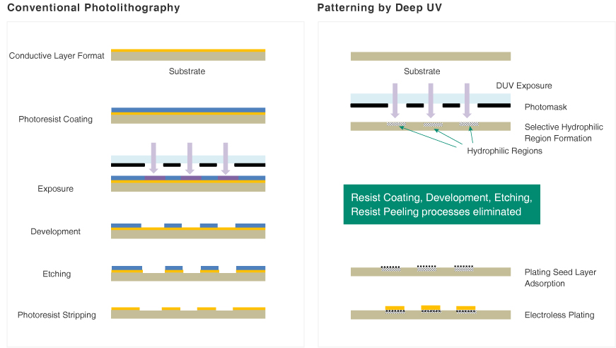
Non-electrolytic copper plating pattern by surface modification patterning
Selective creation of hydrophilic region through photomasks of resin film, etc. The non-electrolytic copper plating pattern is formed after adsorption by just the hydrophilic region of the plating seed layer. Conductors can be formed without resorting to photoresist patterning.
Non-electrolytic copper plating pattern by photosensitive material patterning
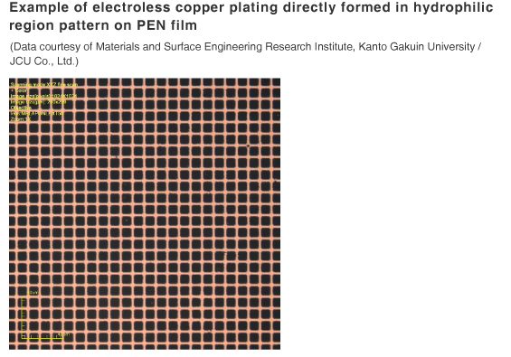
Example of non-electrolytic copper plating pattern using a photosensitive material as a seed layer with absorptivity in the deep UV wavelength region. (Data provided by: Materials & Surface Engineering Research Institute, Kanto Gakuin University, and JCU Corporation)